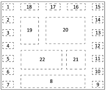
| 1 | SW2 | Test Pin |
| 2 | VIN | Input voltage and input to the LDO regulator. |
| 3 | EN | Enable pin. Turns the MCPF1412M06 ON and OFF. A resistor divider can
be used on this pin to create an external UVLO condition. |
| 4 | PVCC | Input supply for the driver circuits. Connect to VCC. |
| 5 | VCC | Supply voltage. This is used as either a bypass capacitor connection for the
internal LDO or as a connection point for an external bias voltage. |
| 6 | FB | Feedback voltage to the device. Connect the tap of a voltage divider across the
output voltage to this pin to set the output voltage value. |
| 7, 22 | AGND | Signal level ground for the converter and the internal control circuitry. Connect
this to the ground plane of the application. |
| 8 | VOUT | Output voltage of the regulator. Connect output filter capacitors and a 100Ω
resistor from this pin to PGND. |
| 9 | PG | Power Good status indicator. An open drain FET pulls this pin down when Power
Good is not asserted. Connect 49.9 kΩ from this pin to VCC or an external 5V
rail. |
| 10 | ADDR | Address pin. Connect a resistor from this pin to AGND to set the I2C
address of the part. |
| 11 | SYNC | Synchronization input to synchronize the switching to an external source. Connect
to AGND if not used. |
| 12 | SDA | I2C/PMBus data I/O pin. Pull this pin up to the bus voltage with 4.99
kΩ or connect to AGND if not used. |
| 13 | SCL | I2C/PMBus clock pin. Pull this pin up to the bus voltage with 4.99 kΩ
or connect to AGND if not used. |
| 14 | SALERT | SMBAlert# line. Pull this up to bus voltage with a 4.99 kΩ resistor. |
| 15 | SW1 | Optional connection for a capacitor to CB. A 0.1 to 1 μF, 16V or higher rated
MLCC capacitor is recommended. |
| 16, 20, 21 | PGND | Power Ground. This is a separate ground connection for the internal power
devices. Connect to the application power ground plane. |
| 17 | CB | An optional capacitor can be connected from this pin to SW1. |
| 18, 19 | PVIN | Power input terminal for the power switching stage. |