
6 Layout Recommendations
General
The MCPF1412M06 is a highly integrated device requiring minimal external components, which simplifies PCB layout. However, to ensure optimal performance, adhere to these general PCB design guidelines:
- Place bypass capacitors, including input/output capacitors and the VCC bypass capacitor (if used), as close as possible to the MCPF1412M06 pins.
- Sense the output voltage with a separate trace directly from the output capacitor.
- For thermal dissipation, connect the PGND pad to the power ground plane using vias. Copper-filled vias are preferred, but plated-through-hole vias are acceptable if not covered with solder mask. VIPPO techniques are also acceptable.
- Use an adequate number of vias to connect between layers, especially for power traces.
- Connect AGND pins to the PGND copper layer using vias.
- To minimize power losses and improve thermal dissipation, use wide copper polygons for input and output power connections.
Thermal
The MCPF1412M06 has undergone thermal testing and modeling in line with JEDEC standards JESD 51-2A and JESD 51-8. Testing was conducted using a 4-layer application PCB, featuring thermal vias beneath the device to aid in cooling.
The MCPF1412M06 has two main heat sources:
• The power MOSFET section of the IC
• The inductor
The IC is effectively coupled to the PCB, which serves as its primary cooling pathway. While the inductor is also connected to the PCB, its main cooling mechanism is through convection. Ultimately though, both heat sources dissipate heat through convection. The PCB functions as a heat spreader or, to some extent, a heat sink.

Figure 6-2 illustrates the thermal resistances in the MCPF1412M06, described as follows:
- θJA represents the measure of natural convection from the assembled test sample within a confined enclosure of approximately 30 x 30 x 30 cm. The air in this environment is passive, with movement occurring solely due to convection from the device under test.
- θJCbottom indicates the heat flow from the IC to the bottom of the package, where it is well-coupled. The testing method follows the procedure outlined in JESD 51-8, with the test PCB clamped between cold plates at specified distances from the device.
- θJCtop theoretically represents the heat flow from the IC to the top of the package. However, this is not applicable to the MCPF1412M06 for two reasons: firstly, it is not the primary conduction path of the IC, and more importantly, the inductor is positioned directly over the IC. Since the inductor generates a similar amount of heat as the IC, a meaningful value for junction-to-case (top) cannot be determined.
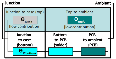
The thermal resistance values are as follows:
- θJA = 20.5°C/W
- θJCbottom = 5.5°C/W
While these values provide a comparison of the MCPF1412M06 with similar POL products under identical conditions and specifications, they are not sufficient for predicting overall thermal performance. For precise modeling of the device’s interaction with its environment, Computational Fluid Dynamics (CFD) simulation software is required to simultaneously calculate the combined effects of conduction and convection.