2.8.2 Via
(Ask a Question)The following are the via placement steps:
- The target impedance of vias are designed
by adjusting the pad clearance (anti-pad size). Field solver must be used to optimize the
via according to the stack-up.
Figure 2-28. Via Illustration1 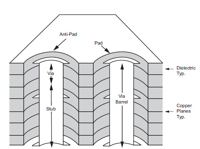 Important: Simonovich, E. Bogatin, Y. Cao, Method of Modeling Differential Vias, White Paper, Jan 2011
 - Number of vias on different traces must be avoided or minimized. SerDes signals must be routed completely on a single layer with the exception of via transitions from component layer to the routing layer (3-via maximum).
The length of via stub must be minimized by back drilling the vias, or by routing the signals from near top to near bottom layer, or else blind or buried vias can be used. Using blind-vias or back drilling is a good method to eliminate via stubs and reduce reflections.
The stub length must be kept below 100 mils, if the data rate is 2.5 Gbps and 40 mils for 5 Gbps.
If feasible, non-functional pads must be removed. Non-functional pads on via are the pads where no trace is connected. This reduces the via capacitance and stub effect of pads.
Figure 2-29. Non-Functional Pads of Via 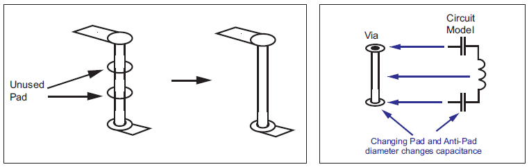
The tight via to via pitch is practical to reduce the cross talk effect, as shown in the following figure.
Figure 2-30. Via-to-Via Pitch 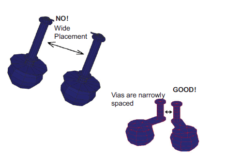
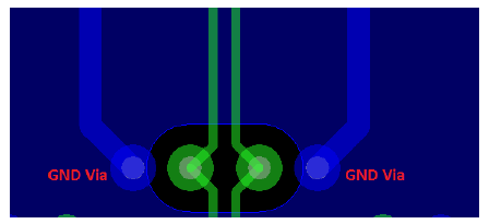
Symmetrical ground vias (return vias) must be used to reduce discontinuity for Common mode signal component, as shown in the following figure. Common mode of part of the signal requires continuous return path RX to TX and GND. Return vias help in maintaining the continuity.
Figure 2-31. GND Via or Return Via