2.8.1.1 Differential Traces
(Ask a Question)A well designed differential trace not must have the following qualities:
- Mismatch in impedance
- Insertion loss and return loss
Skew within the differential traces
The following points need to be considered while routing the high-speed differential traces to meet the preceding qualities.
- The traces must be routed with tight length
matching (skew) within the differential traces. Asymmetry in length causes conversion of
differential signals in Common mode signals. The differential pair must be routed such that
the skew within differential pairs is less than 5 mils. The length match must be used by
matching techniques, as shown in the following figure.
Figure 2-24. Skew Matching 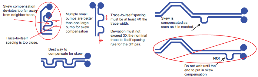
The length of differential lanes must be matched within the TX and RX group. This is applicable only to specific protocols like XAUI and so on.
Route differential pairs symmetrically into and out of structures, as shown in the following figure.
Figure 2-25. Example of Asymmetric and Symmetric Differential Pairs Structure 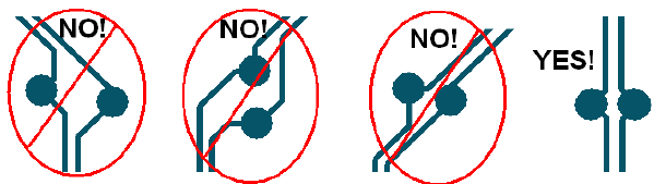
Skin effect dominates as the speed increases. To reduce the skin effect, width of the trace has to be increased (loosely coupled differential traces). Increase in trace width causes increase in dielectric losses. To reduce the dielectric loss, use low Dissipation Factor (Df) PCB materials like Nelco 4000-13. This is approximately double the cost of FR4 PCB material, but can provide increased eye-opening performance when longer trace interconnections are required. Remember to maintain 100 Ω differential impedance. Need to consider this if the data rate is 5 Gbps and above.
Far end cross talk is eliminated by using stripline routing. However, routing in stripline causes more dielectric loss and more variation in the impedance. Cross talk affects only when there is a high density routing. It is better to route as microstrip, if there is enough space between differential pairs (> 4 times the width of the conductor) to reduce dielectric loss. Simulations are recommended to see the best possible routing.
2116 or 2113 glass weaving PCB materials must be used to avoid the variations in the impedances. Zig-zag routing must be used instead of straight line routing to avoid glass weaving effect on impedance variations, as shown in the following figure. Instruct the fabrication vendor to use these PCB materials before manufacturing.
Figure 2-26. Zig-Zag Routing 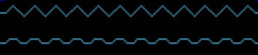
These traces must be kept away from the aggressive nets or clock traces. For example, on M2S050T devices, the SerDes and DDR traces must not be adjacent to each other.
Separation between the coupled differential trace pairs must be 1x. Spacing between channels must be > 3x separation. Trace stubs must be avoided. The stub length must not exceed 40 mils for 5 Gbps data rate.
The trace lengths must be kept as small as possible.
Use low roughness, that is, smooth copper. As the speed increases insertion loss due to the copper, then roughness increases. The attenuation due to skin effect is increased proportional to the square root of frequency. The roughness courses this loss proportional to frequency. Instruct the PCB fabrication house to use smooth copper, if the frequency exceeds 2 Gbps.
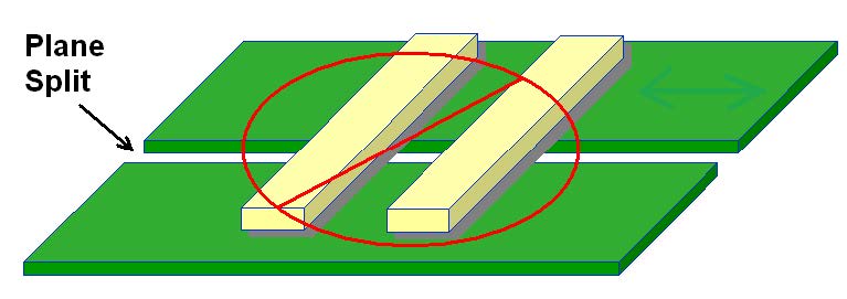
Split reference planes must be avoided. Ground planes must be used for reference for all the SerDes lanes.
Figure 2-27. Ground Planes for Reference