
14.4 Functional Description
SAM L10 Boot ROM Flow
The SAM L10 Boot ROM checks firstly if a debugger is present to enter the Boot Interactive mode which allows the user to perform specific tasks via a debugger connection.

Typical Boot Timings
The delay is given from the release of the CPU reset to the execution of the first instruction of the user code:
| Time to reach User Code |
|---|
| 1.33 ms |
SAM L11 Boot ROM Flow
The SAM L11 Boot ROM sequence consists in performing several security tasks (integrity checks, memories and peripherals security attribution, secure boot...) before starting the application.
The Boot ROM checks firstly if a debugger is present to enter the Boot Interactive mode which allows the user to perform specific tasks via a debugger connection.

Device Integrity Checks
- The User Row CRC
(USERCRC) which is located in the NVM User Row (UROW) at:
[0x80401C:0x80401F]:
UROW Offset Bit Position Name 0x1C-0x1F 255:224 USERCRC - The Boot Configuration
Row CRC (BOCORCRC) which is located in the NVM Boot Configuration Row
(BOCOR) at: [0x80C008:0x80C00B]:
BCOR Offset Bit Position Name 0x08-0x0B 95:64 BOCORCRC
User Row CRC (USER CRC)
USERCRC allows to check the following fuses parameters integrity:
- AS, ANSC, DS, RS
- URWEN
- NONSECA, NONSECB, NONSECC
USERCRC is the CRC of the NVM User row area which starts from 0x00804008 and finish at 0x0080401B (bit 64 to bit 223):
| Offset | Bit Pos. | Name | |||||||
|---|---|---|---|---|---|---|---|---|---|
| 0x08 | 71:64 | AS | |||||||
| 0x09 | 79:72 | Reserved | ANSC | ||||||
| 0x0A | 87:80 | Reserved | DS | ||||||
| 0x0B | 95:88 | Reserved | RS | ||||||
| 0x0C | 103:96 | Reserved | URWEN | ||||||
| 0x0D-0xF | 127:104 | Reserved | |||||||
| 0x10-0x13 | 159:128 | NONSECA | |||||||
| 0x14-0x17 | 191:160 | NONSECB | |||||||
| 0x18-0x1B | 223:192 | NONSECC | |||||||
Boot Configuration Row CRC (BOCORCRC)
BOCORCRC allows to check the following fuses parameters integrity:
- BS, BNSC
- BOOTOPT
- BOOTPROT, BCWEN, BCREN
BOCORCRC is the CRC of the NVM Boot Configuration row area, which starts from 0x0080C000 and finish at 0x00800C007 (bit 0 to bit 63).
| Offset | Bit Pos. | Name | |||||||
|---|---|---|---|---|---|---|---|---|---|
| 0x00 | 7:0 | Reserved | |||||||
| 0x01 | 15:8 | BS | |||||||
| 0x02 | 23:16 | Reserved | BNSC | ||||||
| 0x03 | 31:24 | BOOTOPT | |||||||
| 0x04 | 39:32 | BOOTPROT | |||||||
| 0x05 | 47:40 | Reserved | |||||||
| 0x06 | 55:48 | Reserved | BCREN | BCWEN | |||||
| 0x07 | 63:56 | Reserved | |||||||
- This will allow, if a debugger is connected, to put the device in the highest debug access level mode (DAL = 2) by issuing a Chip Erase command . Once in that mode, it is possible for a programming tool to reprogram the NVM Rows.
- When the check fails and no debugger is connected, the part will reset and restart the check sequence again.
CRC Computation and Programming
The CRCs needs to be recalculated and updated in their respective NVM row as soon as a data from any of the checked regions is changed.
- Width = 32 bits
- Polynomial = 0x04C11DB7 (Poly)
- Initial Value = 0xFFFFFFFF (Init)
- Input Data is reflected (RefIn)
- Output Data is reflected (RefOut)
- No XOR is performed on the output CRC (XorOut)
Example: the DSU CRC of 0x31, 0x32, 0x33, 0x34, 0x35, 0x36, 0x37, 0x38, 0x39 is 0x340BC6D9
Memories and Peripherals Configurations Initialization
For SAM L11 devices, memories and peripherals security attributions are done by reading the different fuses values from the NVM User (UROW) and Boot Configuration (BOCOR) rows.
- Set memory security attribution according to AS, ANSC, DS, RS, BS, BSNC and BOOTPROT fuses
- Set peripherals security attribution according to NONSECA, NONSECB and NONSECC fuses
Secure Boot
- The Secure Flash (BS
region) which is composed by:
- The Secure Flash (BOOT region)
- The Non-Secure Callable Flash (BOOT region)
- And the NVM Boot Configuration row (BOCOR)
| BOOTOPT | Verified Areas | Verification Method |
|---|---|---|
| 0 | None | - |
| 1 |
Secure Flash (BS region) + NVM BOCOR row | SHA-256 |
| 2 or 3 |
Secure Flash (BS region) + NVM BOCOR row | SHA-256 with BOOTKEY (defined in BOCOR) |
If the verification fails, the Boot ROM will report the error to the DSU peripheral and will enter the Boot Interactive mode. This will allow, if a debugger is connected, to put the device in the highest debug level access mode (DAL = 2) by issuing a Chip Erase command. Once in that mode, it is possible for a programming tool to reprogram the different memory regions and/or NVM rows.
When verification fails and no debugger is connected, the part will reset and restart the integrity checks sequences again.
Hash algorithm (SHA-256) Verification Method
The verifications are done using the standard SHA256 hash algorithm.
SHA256 with BOOTKEY Variant
To prevent unauthorized change of the bootloader code, the digest computation can be slightly modified to require a key to produce a valid digest.
When SHA with BOOTKEY is selected (BOOTOPT=2 or =3), the digest computation (for both Secure Flash (BS region) and NVM BOCOR row) starts by processing the secure boot key (BOOTKEY) data twice, then proceeds with the rest of data.
| BOCOR Offset | Bit Position | Name |
|---|---|---|
| 0x50-0x6F | 895:640 | BOOTKEY |
BS Verification
When BOOTOPT>0, the bootloader authentication starts allowing a secure bootloader code to be protected against inadvertent or malicious changes.
The digest is computed on the Secure Flash (BOOT region) and the Non-Secure Callable Flash (BOOT region).
The digest reference value for this area is stored at the end of the Secure Flash (BOOT region), just before the Non-Secure Callable Flash (BOOT region).

BOCOR Verification
| BOCOR Offset | Bit Position | Name |
|---|---|---|
| 0xE0-0xFF | 2047:1792 | BOCORHASH |
Typical Boot Timings
Depending on the boot authentication options, the Boot ROM will require a certain time to complete its different tasks.
The delay is given from the release of the CPU reset to the execution of the first instruction of the user code.
| Boot options | Time to reach User Code |
|---|---|
| BOOTOPT=0 | 2.30 ms |
| BOOTOPT=1, BS=0x40 | 207 ms |
| BOOTOPT=1, BS=0x80 | 409 ms |
| BOOTOPT=2, BS=0x40 | 209 ms |
| BOOTOPT=2, BS=0x80 | 411 ms |
Debug Access Levels
- DAL2: Highest debug level access with no restrictions in term of memory and peripheral accesses.
- DAL0: No access is authorized except with a debugger using the Boot ROM Interactive mode.
The possible transitions between each debug access level are described below:

The SAM L11 has three possible debug access levels (DAL):
- DAL2: Highest debug level access with no restrictions in term of memory and peripheral accesses.
- DAL1: Access is limited to the Non-Secure memory regions. Secure memory regions accesses are forbidden.
- DAL0: No access is authorized except with a debugger using the Boot ROM Interactive mode.
The possible transitions between each debug access level are described below:

For security reasons, increasing the Debug Level Access is only possible during Boot ROM execution and will be always preceded by a specific chip erase depending on the Debug Access Level.
Chip Erase
For SAM L10, the chip erase command does not require a key.
For SAM L11, the chip erase commands are protected with keys (CEKEYx) defined in the NVM BOCOR row.
| SAM L11 | SAM L10 | |||
|---|---|---|---|---|
| Boot ROM Command | ChipErase_NS (CE0) | ChipErase_S (CE1) | ChipErase_ALL (CE2) | ChipErase (CHIPERASE) |
| Key Requirement | Yes (CEKEY0) | Yes (CEKEY1) | Yes (CEKEY2) | No |
| Flash (BOOT region) BOOTPROT (BS+BNSC+BNS) | No | No | Yes | No |
| Flash (APPLICATION region) | - | - | - | Yes |
| Data Flash | - | - | - | Yes |
| Secure Flash (AS region) | No | Yes | Yes | - |
| Non-Secure Flash (APPLICATION region) | Yes | Yes | Yes | - |
| Secure Data Flash (DS) | No | Yes | Yes | - |
| Non-Secure Data Flash | Yes | Yes | Yes | - |
| NVM User Row (UROW) | No | No | Yes | No |
| NVM Boot Configuration Row (BOCOR) | No | No | Yes | No |
| Volatile Memories | Yes | Yes | Yes | Yes |
| Debugger Access Level after reset | 2 (if DAL was 2) else 1 | 2 (if DAL was 2 or BS==0) else 1 | 2 | 2 |
Boot ROM Interactive Mode
The interactive mode allows the user to perform several actions on the device during the Boot ROM execution via a debugger connection.
Enter Interactive Mode (CMD_INIT)
This command allows launching the Boot Interactive command mode of the Boot ROM.
When CRSTEXT is cleared, CPU starts Boot ROM Interactive mode execution. After a small delay (5ms advised), the debugger must check if the Boot ROM has not flagged any errors by checking the BCCD1 bit in DSU.STATUSB register.
If errors are reported, the debugger can get the error type by checking the DSU.BCC1 register from the DSU external address space.
If no error is reported, the debugger writes the CMD_INIT command to DSU.BCC0 register to request Boot ROM Interactive mode entry. When command is successful, Boot ROM will place the “SIG_COMM” status in DSU.BCC1 register.
CMD_INIT

Exit Interactive Mode (CMD_EXIT)
This command allows exiting the Boot Interactive mode.
- The Application
- The CPU Park Mode
CMD_EXIT


System Reset Request (CMD_RESET)
This command allows resetting the system using a system reset request. Since the reset is executed immediately after receiving the command, no reply is sent to the debugger.
After reset, the CPU executes the Boot ROM code from the beginning
Chip Erase (CMD_CHIPERASE) - SAM L10 only
CMD_CHIPERASE command erases the entire device except BOOT area, and reverts to Debug Access Level 2.
CMD_CHIPERASE (SAM L10 only)

Chip Erase (CMD_CEx) - SAM L11 only
CMD_CEx commands are used to erase specific part of the device and to increase the Debug Access Level.
CMD_CEx (SAM L11 only)

NVM Memory Regions Integrity Checks (CMD_CRC)
The Boot ROM provides a way to check the integrity of the embedded non-volatile memories which may be of interest in case of a failure analysis.
This requires the user to place tables describing the memory area to be checked with their expected CRC values.
CRC Table format
| Description | Header | Start Address (1) | Size in bytes (2) | Expected value (3) |
|---|---|---|---|---|
| Field | HDR | ADDR | SIZE | REFVAL |
| Offset | 0x0 | 0x4 | 0x8 | 0xC |
| Value | 0x43524349 | 0x00000000 | 0x100 | 0xAABBCCDD |
Note 1: ADDR must be a multiple of 4 (Only ADDR[31:2] are used).
Note 2: SIZE must be a multiple of 4 (Only SIZE[31:2] are used).
Note 3: The expected value is the computed CRC32 value of the memory target.
Requirements
- Each table occupies 16 bytes in memory.
- The table must start at a 16byte aligned address. (i.e. 0xXXXXXXX0)
- The table must be
placed in the same memory region as its target memory range. (i.e. a
table placed in the Secure Flash (APPLICATION region) can only
target Secure Flash (APPLICATION region) memory addresses).Note: There are two exceptions to this rule:
- For SAM L10: all non-volatile memories are considered as a single region (e.g. a table located in Data Flash can target Flash)
- For SAM L11: ANSC and BNSC regions are considered to belong to the same region as their “parent” region: AS for ANSC and BS for BNSC.
CRC Command Key
| BOCOR Offeset | Bit Position | Name |
|---|---|---|
| 0x40-0x4F | 639:512 | CRCKEY |
Just like the ChipErase keys, the key can be set to all 0s to prevent any access to the command.
CMD_CRC

Random Session Key Generation (CMD_DCEK) - SAM L11 only
This command allows using a challenge-response scheme to prevent exposure of the keys in clear text on the debugger communication lines.
The different keys sent by the debugger during the Boot ROM for Chip Erase (CMD_CEx) and CRC (CMD_CRC) commands execution are:
- CRCKEY for CMD_CRC command
- CEKEYx for CMD_CEx commands
The random challenge value is generated using the TRNG of the device. It is generated once the CMD_DCEK is received and communicated to the debugger.
The next CMD_CEx or CMD_CRC commands will expect the key value to be replaced by the computed response corresponding to the challenge.
The challenge value is valid only for the next CMD_CEx/ CMD_CRC command.
Before sending a new CMD_CEx/ CMD_CRC command, a CMD_DCEK shall be used to re-enable the challenge-response scheme a get a new challenge value.
On the debugger side, the response shall be computed using the following algorithm:
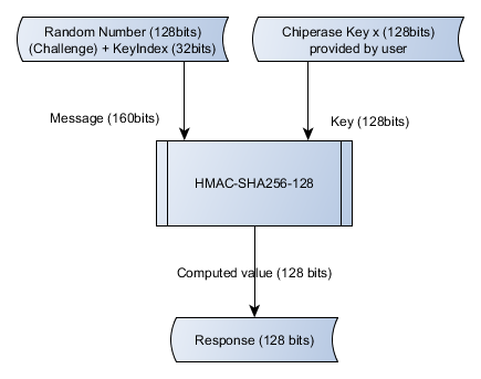
Where KeyIndex is:
- 0 for ChipErase_NS
- 1 for ChipErase_S
- 2 for ChipErase_ALL
- 3 for CRC Command
- HMAC is described in FIPS PUB 198-1
- The hash used for HMAC is SHA-256
- The output of the HMAC-SHA256 is truncated to obtain an HMAC-SHA256-128 as explained in RFC4868
CMD_DCEK (SAM L11 only)

NVM Rows Content Checks (CMD_RAUX)
The Boot ROM provides a way to check the content of the NVM rows.
When device is secured (DAL0), the fuse configuration can still be read by the debugger using the Read Auxiliary command (CMD_RAUX).
| Area | Start address | End address |
|---|---|---|
| User row (UROW) | 0x00804000 | 0x0080401F |
| Software Calibration row | 0x00806020 | 0x0080602F |
| Temperature Log row | 0x00806038 | 0x0080603F |
- Boot Configuration row (BOCOR) is not accessible by the Read Auxiliary Row command.
CMD_RAUX

Note: After the CMD_RAUX is sent, the debugger can read multiple data, the read loop is exit when an out of range address is sent.
Boot Interactive Mode Commands
| Command Name | Description | Command prefix | Command |
|---|---|---|---|
| CMD_INIT | Entering Interactive Mode | 0x444247 | 55 |
| CMD_EXIT | Exit Interactive Mode | 0x444247 | AA |
| CMD_RESET | System Reset Request | 0x444247 | 52 |
| CMD_CE0 | ChipErase_NS for SAM L11 | 0x444247 | E0 |
| CMD_CE1 | ChipErase_S for SAM L11 | 0x444247 | E1 |
| CMD_CE2 | ChipErase_ALL for SAM L11 | 0x444247 | E2 |
| CMD_CHIPERASE | ChipErase for SAM L10 | 0x444247 | E3 |
| CMD_CRC | NVM Memory Regions Integrity Checks | 0x444247 | C0 |
| CMD_DCEK | Random Session Key Generation for SAM L11 | 0x444247 | 44 |
| CMD_RAUX | NVM Rows Integrity Checks | 0x444247 | 4C |
Boot Interactive Mode Status
| Status Name | Description | Status prefix | Status coding |
|---|---|---|---|
| SIG_NO | No Error | 0xEC0000 | 00 |
| SIG_SAN_FFF | Fresh from factory error | 0xEC0000 | 10 |
| SIG_SAN_UROW | UROW checksum error | 0xEC0000 | 11 |
| SIG_SAN_SECEN | SECEN parameter error | 0xEC0000 | 12 |
| SIG_SAN_BOCOR | BOCOR checksum error | 0xEC0000 | 13 |
| SIG_SAN_BOOTPROT | BOOTPROT parameter error | 0xEC0000 | 14 |
| SIG_SAN_NOSECREG | No secure register parameter error | 0xEC0000 | 15 |
| SIG_COMM | Debugger start communication command | 0xEC0000 | 20 |
| SIG_CMD_SUCCESS | Debugger command success | 0xEC0000 | 21 |
| SIG_CMD_FAIL | Debugger command fail | 0xEC0000 | 22 |
| SIG_CMD_BADKEY | Debugger bad key | 0xEC0000 | 23 |
| SIG_CMD_VALID | Valid command | 0xEC0000 | 24 |
| SIG_CMD_INVALID | Invalid command | 0xEC0000 | 25 |
| SIG_ARG_VALID | Valid argument | 0xEC0000 | 26 |
| SIG_ARG_INVALID | Invalid argument | 0xEC0000 | 27 |
| SIG_CE_CVM | Chip erase error: CVM | 0xEC0000 | 30 |
| SIG_CE_ARRAY_ERASEFAIL | Chip erase error: array erase fail | 0xEC0000 | 31 |
| SIG_CE_ARRAY_NVME | Chip erase error: array NVME | 0xEC0000 | 32 |
| SIG_CE_DATA_ERASEFAIL | Chip erase error: data erase fail | 0xEC0000 | 33 |
| SIG_CE_DATA_NVME | Chip erase error: data NVME | 0xEC0000 | 34 |
| SIG_CE_BCUR | Chip erase error: BOCOR, UROW | 0xEC0000 | 35 |
| SIG_CE_BC | Chip erase error: BC check | 0xEC0000 | 36 |
| SIG_BOOT_OPT | BOOTOPT parameter error | 0xEC0000 | 40 |
| SIG_BOOT_ERR | Boot image digest verify fail | 0xEC0000 | 41 |
| SIG_BOCOR_HASH | BOCOR hash error | 0xEC0000 | 42 |
| SIG_CRC_BADTBL | Bad CRC table | 0xEC0000 | 50 |
| SIG_SECEN0_ERR | PAC or IDAU cfg check failure | 0xEC0000 | 60 |
| SIG_SECEN1_ERR | PAC or IDAU cfg check failure | 0xEC0000 | 61 |
| SIG_EXIT_ERR | Exit: BC or check error | 0xEC0000 | 70 |
| SIG_HARDFAULT | Hardfault error | 0xEC0000 | F0 |
| SIG_BOOTOK | Boot ROM ok to exit | 0xEC0000 | 39 |
CPU Park mode
This mode allows the debugger to get access to the resources of the device during Boot ROM execution while the CPU is trapped in a while loop. The debug access level when entering that mode corresponds to the DAL value which is programmed in the device.
This mode is reached by sending the Exit command (CMD_EXIT) without clearing the DSU.STATUSA.BREXT bit to the Boot ROM.
As soon as the BREXT bit is cleared, the device exits this state and performs a system reset.
At this point, the MPU is still enabled and prevents software execution elsewhere than in Boot ROM region.
If the host needs to run software on the device, MPU shall be disabled by accessing the Cortex-M23 MPU CTRL register with the debugger.