
2.6 HSIO/GPIO Bank Initialization
(Ask a Question)Unused GPIO and HSIO banks can be left powered down or powered up. During the device power-up, the used GPIO and HSIO banks are simultaneously powered up along with all the other power supplies. All banks are initialized automatically with Flash configuration bits when the fabric is powered up. All powered-up user I/Os (HSIO/GPIO) also normally go through an initial PVT I/O calibration (auto calibration) on power-up. Bank 3 (dedicated device I/O) does not calibrate, and transceiver I/Os have unrelated dedicated calibration circuitry.
The time at which I/Os are functional depends on a combination of the following:
- Device boot
- Ramp-up time of the power applied to the I/O banks
- Calibration time of I/Os (For example, DDR interfaces)
I/Os are functional after the power applied to I/O banks exceeds the minimum threshold levels. Prior to I/O calibration, the I/Os are functional but may not operate to the expected performance levels. This is due to the maximum calibration setting in the I/O calibration default configuration (strongest calibration drives strength and lowest, termination value). This configuration persists until the I/O calibration process completes. When enabled, the I/O calibration process occurs automatically. Auto calibration is enabled on every bank by default in the Libero SoC tool. Completion of the bank’s auto calibration enable process can be monitored via the AUTOCALIB_DONE signal from the PF_INIT_MONITOR IP and PFSOC_INIT_MONITOR IP. To determine the completion of a specific bank calibration, monitor the BANK_x_CALIB_STATUS.
Bank I/O auto calibration and voltage ramp time can be configured using the Libero SoC I/O Editor as shown in the following image.
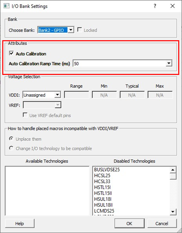
Each I/O bank has an Auto Calibration check box to enable calibration. However, auto calibration is controllable at the device level only. All banks are either auto calibrated or no banks are auto calibrated.
- Auto calibration is enabled on all banks by checking the bank’s Auto Calibration check box on at least one bank that has at least 1 user I/O assigned to it. It enables auto calibration on all I/O banks.
- Disabling auto calibration is done by clearing the Auto Calibration check box on all banks.
Selecting the Auto Calibration check box on a specific bank enables the auto calibration ramp time setting for the specific bank. This ramp time must be configured to a delay time that allows the bank power rails, VDDI/VDDAUX, sufficient time to fully ramp and stabilize. With auto calibration enabled, any bank that has the Auto Calibration check box cleared will be enabled to calibrate directly after the calibration of all the banks with the Auto Calibration check box selected. Once enabled, these banks calibrate when the bank VDDI/VDDAUX exceeds the minimum threshold levels. This scenario can result in an inaccurate bank calibration if these voltage rails are still ramping up to full operating levels while calibration is in progress. To obtain an accurate calibration on such I/O banks, it is necessary to initiate a recalibration. For information about I/O recalibration, see I/O Recalibration.
If a designer requires the I/Os to be usable immediately upon completion of device boot, the auto calibration ramp time should be set sufficiently short and bank voltage ramp time sufficiently fast to meet boot time goals.
The user can also apply slow or delayed auto calibration ramp time on I/O banks to delay the time until which the I/Os are usable.
To time bound the auto-calibration process, a global auto calibration timeout exists. The setting of this value is shown in the following figure.
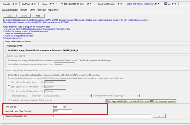
Configure this timeout option based on selected GPIO or HSIO in the user design. Auto Calibration Time Out must be configured to a time greater than the time it takes for all calibration enabled banks to ramp up to their stable operating bank voltages. This timeout delay starts after TFAB_READY. For more information, see PolarFire FPGA Datasheet , RT PolarFire FPGA Datasheet , PolarFire SoC FPGA Datasheet , or RT PolarFire SoC FPGA Datasheet . Once the global Auto Calibration Timeout time expires, all uncalibrated banks will have their auto calibration engines enabled. This is possible if, for example, a bank’s VDDI/VDDAUX do not start ramping until after this global timeout. In this scenario, calibration then starts as soon as bank VDDI/VDDAUX reach their minimum operating voltage threshold. This could result in an inaccurate bank calibration if these voltage rails are still ramping up to full operating levels while calibration is in progress. To obtain an accurate calibration on such I/O banks, it is necessary to initiate a recalibration using the recalibration interfaces available from the PF_INIT_MONITOR IP and PFSOC_INIT_MONITOR IP once the bank voltages stabilize at their operating levels. (See I/O Recalibration.)
User logic in the fabric should be implemented to monitor the state of the I/O banks to know when they are usable. The PF_INIT_MONITOR IP and PFSOC_INIT_MONITOR IP assert BANK_#_CALIB_STATUS and BANK_#_VDDI_STATUS signals to the fabric. BANK_#_CALIB_STATUS can be used by the user logic to determine if the calibration completes for each I/O bank. BANK_#_VDDI_STATUS signal can be used to monitor VDDI supply on specific I/O banks. The assertion of AUTOCALIB_DONE indicates that the auto calibration sequence has completed where all calibration engines are enabled. To determine if a bank has completed calibration, monitor BANK_#_CALIB_STATUS.
The recommendations for configuring the calibration subsystem are as follows:
- The overall goal must be to ensure that the bank voltages reach their stable operating voltage levels prior to the bank ramp time expiration to assure proper calibration. If this cannot be met for a particular bank, prior to expiration of the global auto calibration timeout, then the user must manually execute re-calibration on the bank once VDDI/VDDAUX are at their stable operating levels.
- For banks that power up during the normal chip boot-up: Enable auto calibration and configure the bank's auto calibration ramp time to a value that allows the bank's VDDI/VDDAUX to stabilize to the desired operating voltage.
- For unused/unpowered banks: Disable auto calibration. This will enable auto calibration on these banks once all enabled banks complete calibration. This is to avoid the auto-calibration process to run until the global auto calibration timeout expires, improving the chip boot time.
- For banks that power-up long after device boot time or banks that experience power cycles during normal operation: Disable auto calibration and manually execute dynamic re-calibration when the bank’s VDDI/VDDAUX stabilizes to the desired operating voltage (see I/O Recalibration). This is to avoid the auto-calibration process to run until the global auto calibration timeout expires, improving the chip boot time.
- Configure the global auto calibration timeout to a value greater than the time it takes for all calibration enabled banks to ramp up to their stable operating bank voltages.