
2.3 Design and Memory Initialization
(Ask a Question)After the device boot process completes, the fabric RAM blocks (LSRAMs and µSRAMs) are initialized to zero by default. In the PolarFire family of devices, the fabric RAM blocks can be initialized with known values, if desired. PCIe and XCVR blocks used in the design are initialized with the user configuration data at power-up. The System Controller performs the design and memory initialization during the power-up sequence. The memory initialization data can be stored in µPROM, sNVM, or an external SPI Flash. The storage location of the initialization data is selected during the Libero design flow. The initialization data can be encrypted for storing in external SPI Flash.
The following figure shows the sequence in which the fabric, PCIe, Transceiver, LSRAMs, and µSRAMs are automatically initialized. The sequence is customized depending on the resources instantiated in the user design. For example, the PCIE_INIT_DONE will not assert if the user design does not contain PCIe. As a result, the sequence skips the PCIe initialization and moves to the next step. At this stage in the PolarFire SoC and RT PolarFire SoC FPGA devices, the MSS remains in reset.
In Libero SoC, memory initialization can be done using any of the following methods:
- Importing the content file using the fabric RAMs tab of the Configure Design Initialization Data and Memories option after Place and Route is performed. For more information, see How To Set Up Design and Memory Initialization.
- Importing the content file using the LSRAM and µSRAM Configurator before Place and Route. For more information, see RAM Initialization Before Place and Route.
The user can monitor the design initialization status using the Initialization Monitor.
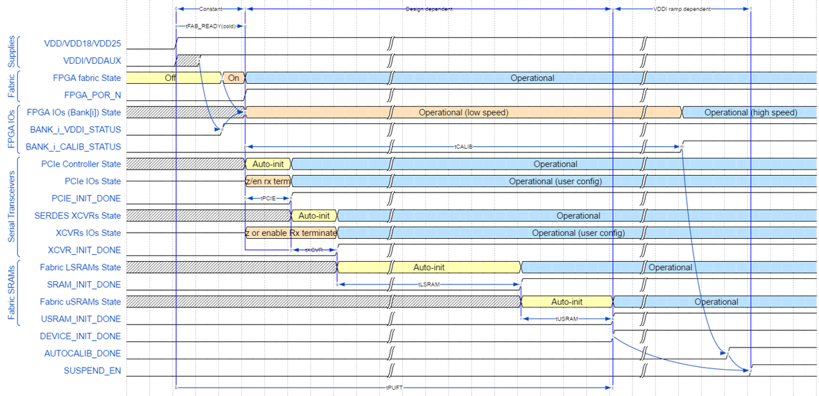
The total power-up to functional time is as shown in the following equation:
PUFT is variable depending on the design configuration.
For more information about typical PUFT, see the respective PolarFire FPGA Datasheet , RT PolarFire FPGA Datasheet , PolarFire SoC FPGA Datasheet , or RT PolarFire SoC FPGA Datasheet .
- Power-up To Functional Time is based on the case where VDDI/VDDAUX of I/O banks are powered either before or after VDD/VDD18/VDD25. The I/O bank enable time is measured from the assertion time of VDD/VDD18/VDD25. If VDDI/VDDAUX of IO banks are powered sufficiently after VDD/VDD18/VDD25, then the I/O bank enable time is measured from the assertion of VDDI/VDDAUX. In this case, I/O operation is indicated by the assertion of BANK_#_VDDI_STATUS, rather than being measured relative to FABRIC_POR_N negation.
- The assertion of AUTOCALIB_DONE can occur before or after the assertion of DEVICE_INIT_DONE. The time taken for the assertion of AUTOCALIB_DONE depends on:
- The time when VDDI/VDDAUX is up after VDD/VDD18/VDD25 is powered on.
- The ramp times of VDDI of each I/O bank designated for auto-calibration.
- How much auto-initialization is to be performed for the PCIe, SerDes transceivers and fabric LSRAMs.
- If any of the I/O banks specified for auto-calibration do not have their VDDI/VDDAUX powered on within the auto-calibration timeout window, then it auto-calibrates whenever VDDI/VDDAUX is subsequently powered on. In this scenario, calibration will start as soon as VDDI/VDDAUX reach their minimum operating voltage threshold. This could result in an inaccurate calibration if these voltage rails are still ramping up to full operating voltage levels. To obtain an accurate calibration on such I/O banks, it is necessary to initiate a re-calibration using the recalibration interfaces available from the PolarFire Initialization Monitor IP.
- User logic in the FPGA fabric can determine if a given I/O bank has completed its auto-calibration or not by means of looking at the corresponding calib_status signal to the fabric known as BANK#_CALIB_STATUS in SmartDesign.
- SUSPEND_EN asserts (if the suspend mode is enabled) about 100 system controller clock cycles after the assertion of DEVICE_INIT_DONE or AUTOCALIB_DONE.
- PolarFire family of devices have built-in tamper detection features to monitor voltage supplies and flags to detect minimum or maximum threshold values. These flags are valid only after design initialization, and not during POR.
The following signals are asserted during the design initialization:
- DEVICE_INIT_DONE: asserted once the execution of design initialization is complete.
- FABRIC_POR_N: de-asserted when the fabric is operational.
- PCIE_INIT_DONE: used by fabric logic to hold PCIe-related fabric logic in reset until the PCIe controller is initialized. PCIE_INIT_DONE is asserted after initializing the PCIe lane instances placed in the PCIe quad. If XCVR lanes are placed in the PCIe capable quad, then XCVR_INIT_DONE is asserted.
- XCVR_INIT_DONE: asserted when the XCVR block is initialized.
- SRAM_INIT_DONE: asserted when the LSRAM blocks are initialized.
- USRAM_INIT_DONE: asserted when the µSRAM blocks are initialized.
- BANK_#_CALIB_STATUS: This signal can be used by user logic to determine if the calibration completes for each IO bank. # denotes the bank number (0, 1, 7, 8, and 9).
- BANK_#_VDDI_STATUS: This signal can be used to monitor the status of the VDDI supply on specific I/O banks. This signal is the output signal from the INIT_MONITOR IP if any of the corresponding bank is selected. # denotes the bank number (0, 1, 7, 8, and 9).
- SRAM_INIT_FROM_SNVM_DONE: asserted when SRAM is initialized from sNVM.
- USRAM_INIT_FROM_SNVM_DONE: asserted when USRAM is initialized from sNVM.
- SRAM_INIT_FROM_UPROM_DONE: asserted when SRAM is initialized from µPROM.
- USRAM_INIT_FROM_UPROM_DONE: asserted when USRAM is initialized from µPROM.
- SRAM_INIT_FROM_SPI_DONE: asserted when SRAM is initialized from SPI.
- USRAM_INIT_FROM_SPI_DONE: asserted when USRAM is initialized from SPI.