4.6 CCC Configuration
(Ask a Question)The PLLs and DLLs present in each CCC are configurable statically using CCC configurator. The CCC configurator provides a visual configuration wizard for a quick and easy way to configure the CCC with desired settings. The CCC configuration set through the configurator defines the power-up state of the CCC. The CCC configurator must be instantiated into the design to use PLL or DLL. A single instantiation of the CCC configurator can be configured as a PLL or DLL. Multiple CCC configurators must be instantiated to use multiple PLLs and DLLs in a design. A design can have up to a maximum of eight PLLs and eight DLLs.
The following figure shows the available configuration options (PLL-Single and DLL) in the CCC Configurator window.

The following figure shows the Clock Options PLL tab of PLL-Single configuration in the Configurator window.

In the Clock Options PLL tab, configure the following parameters:
- Input Frequency: Enter clock frequency of PLL reference clock.
- In Integer mode, frequency ranges from 1 MHz–1250 MHz.
- In Fractional mode, frequency ranges from 10 MHz–1250 MHz.
- Backup Clock: If the design needs a redundant clock of the same frequency, enable the backup clock (REF_CLK_1). The clock switching must be done from the fabric using the REF_CLK_SEL signal.
- Bandwidth: Select the PLL loop bandwidth (Low, Medium-Low, Medium-High, and High) based on jitter and lock time requirements.
- Delay Lines: If the design needs clock delay/phase adjustment, enable delay line in the feedback clock path or backup clock path and select the number of delay steps or taps between 0 to 255.
- Power/Jitter: The VCO operating range can be set for minimum jitter at the output or minimum power consumption.
- Select Maximize VCO for Lowest Jitter to use the highest VCO and FPFD frequencies.
- Select Minimize VCO for Lowest Power to use minimum VCO and FPFD frequencies for low power consumption. In this mode, the lowest first enabled clock output frequency achievable is 200 MHz.
- Feedback Mode: Select PLL feedback mode (Internal, External, or Post-VCO), and feedback clock for the external feedback mode.
- Post-Divider: The configurator uses one of the enabled output clocks as the feedback clock. The selected output clock is shown in the configurator and grayed out.
- External: It exposes the feedback clock port to Fabric. The PLL clock output 0 is selected as the feedback clock.
- Post-VCO: Selects the VCO output as the feedback clock.
- Reset Outputs On PLL Lock: By default, reset on PLL lock is enabled. When this option is disabled, all enabled output clocks start toggling before the PLL is locked. There is no phase relationship between the outputs, and the output clocks are not synchronized with the input reference clock. This feature is available only in Post-VCO feedback mode.
- Features
- Select Integer Mode to use the PLL. When Integer Mode is disabled, PLL is not constrained. PLL finds an Integer or Fractional solution depending on the input reference clock and requested output frequencies.
- Select SSCG Modulation to enable the spread spectrum clock generation. Click the SSCG Modulation tab for more information.
- Select Enable Dynamic Reconfiguration Interface (DRI) to expose the bus interface to the fabric.
- Select Export PowerDown Port to expose the port to fabric.
- PLL Lock: The calculated values for PLL Lock Time and PFD frequency is reported in the GUI.
- PLL Lock Time is calculated as: PFD period * 2Delay_PLL_Lock. The value for Delay_PLL_Lock is fixed at 8 and cannot be changed.
- PFD frequency = PLL input reference clock frequency/PLL reference divider (RFDIV).
The following figure shows the Output Clocks tab of PLL-Single configuration in the Configurator window.
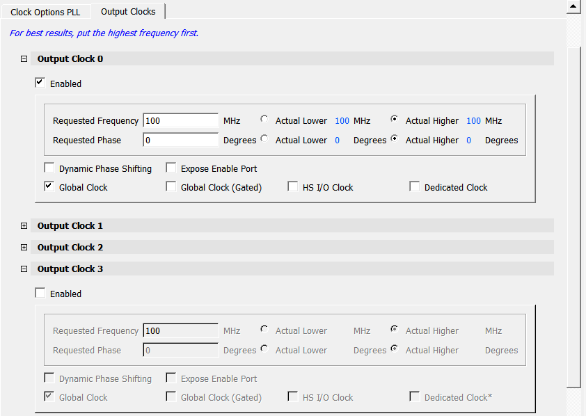
In the Output Clocks tab, configure the following parameters for Output Clock 0, Output Clock 1, Output Clock 2, and Output Clock 3:
- Select Enabled to enable the PLL output clocks.
- Requested Frequency: Ranges from 1 MHz–1250 MHz for both integer and fractional modes. If the configurator is not able to generate an exact match of the requested frequency, it gives two possible frequencies to select from—one above (actual higher) the requested frequency and the other below (actual lower) the requested frequency.
- Requested Phase: Enter the phase shift needed with respect to the reference clock. If the configurator is not able to generate an exact match of the requested phase, it gives two possible phases to select from—one above (actual higher) the requested phase and one below (actual lower) the requested phase.
- Dynamic Phase Shifting: Select to expose the fabric signals for dynamic phase shifting.
The CCC configurator calculates the internal divider and phase settings to generate the requested frequency and phase in the following priority:
- OUT0 frequency
- OUT0 phase
- OUT1 frequency
- OUT1 phase
- OUT2 frequency
- OUT2 phase
- OUT3 frequency
- OUT3 phase
If the user has strict requirement for some frequency or phase, then they need to be allocated first. OUT0 and OUT1 are preferable for high-speed I/O clock as they offer low-latency and jitter.
- Select Expose Enable Port to expose the clock output enable port to the fabric.
- Select PLL output clock connectivity
- Global Clock: To connect the PLL output clock to the global clock network.
- Global Clock (Gated): to connect the PLL output clock to GCLKINT to enable clock gating feature. It exposes OUTx_FABCLK_GATED_x_EN input port and OUTx_FABCLK_GATED_x output port.
- HS I/O Clock: To connect the PLL output clock to a high-speed I/O clock network.
- Dedicated Clock: To connect the PLL output clock to other PLL or DLL in the same CCC, clock dividers, NGMUXs, or preferred clock output pins through dedicated hardwired routing.
The following figure shows the SSCG Modulation tab of PLL-Single configuration in the Configurator window.
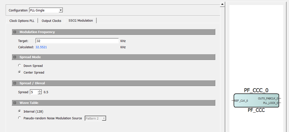
The following parameters are configurable in the SSCG Modulation tab if the SSCG modulation feature is enabled in the Clock Options PLL tab:
- Modulation Frequency: Enter the desired target modulation frequency. The configurator calculates the modulation frequency based on the PLL output frequency and desired modulation value. The calculated value is shown in the configurator.
- Spread Mode: Select Down Spread or Center Spread.
- Spread/Divval: Enter Spread value to compute frequency modulation.
- Wave Table: Select Internal (128) triangular modulation wave table or Pseudo-random Noise Modulation Source with an option to choose between 3 patterns.
The following figure shows DLL configuration settings in Phase Reference Mode.
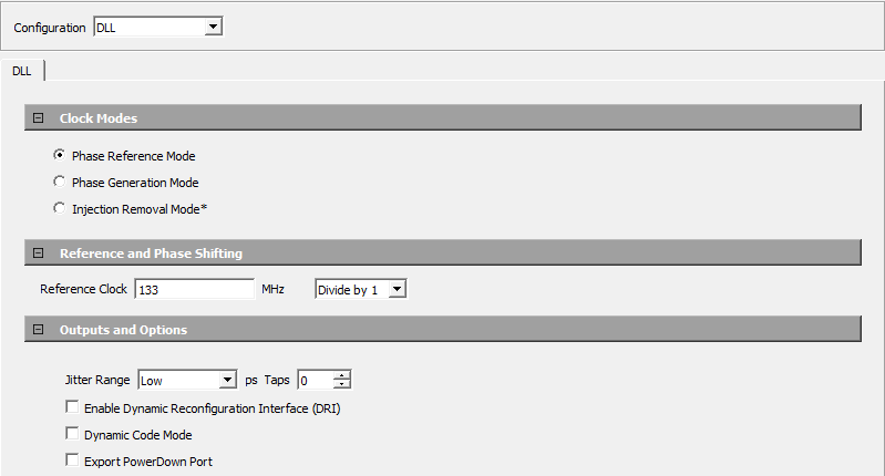
The following parameters are configurable in Phase Reference Mode:
- Reference Clock: Enter the frequency—ranges from 133 MHz–800 MHz.
- Outputs and Options:
- Jitter Range: Select between Low, Medium Low, Medium High, and High.
- Delay Taps: The delay code output can be further adjusted statically by adding or subtracting a number of delay taps. Select between −127 to 127.
- Select Enable Dynamic Reconfiguration Interface (DRI) to expose the bus interface for DLL dynamic configuration.
- Select Dynamic Code Mode to expose the ports for fine tuning the delay code output dynamically.
- Select Export PowerDown Port to expose the port to the fabric.
The following figure shows DLL configuration settings in Phase Generation Mode.
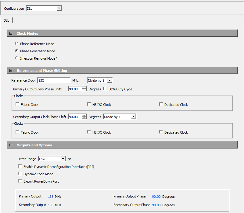
The following parameters are configurable in Phase Generation Mode.
Reference Clock Options
- Frequency: Enter the reference clock frequency—ranges from 133 MHz–800 MHz.
- Division: Select reference clock division value between 1, 2, or 4 as per design requirements.
Primary Output Clock Options
- Phase Shift: If the primary output clock requires phase shifting in multiples of 90°, then select the phase shift from the drop-down list.
- 50% Duty Cycle: Select 50% Duty cycle to regulate the primary output clock for 50% duty cycle.
- Select primary output clock connectivity:
- Fabric Clock: To connect the primary output clock to the global clock network.
- HS I/O Clock: To connect the primary output clock to a high-speed I/O clock network.
- Dedicated Clock: To connect the primary output clock to other DLL or PLL in the same CCC, clock dividers or NGMUXs through dedicated hardwired routing.
Secondary Output Clock Options
- Phase Shift: If the secondary output clock requires phase shifting in multiples of 11.25°, then select the phase shift from the drop-down list.
- 50% Duty Cycle and Clock Division: The secondary clock output can be regulated with a 50% duty-cycle while in 0°, 90°, 180°, 270°, or 360° shift or when divided by 2 or 4.
- Select secondary output clock connectivity:
- Fabric Clock: To connect the primary output clock to the global clock network.
- HS I/O Clock: to connect the primary output clock to a high-speed I/O clock network.
- Dedicated Clock: To connect the primary output clock to other DLL or PLL in the same CCC, clock dividers, or NGMUXs through dedicated hardwired routing.
Outputs and Options
- Jitter Range: Select between Low, Medium Low, Medium High, and High based on the design requirements.
- Select Enable Dynamic Reconfiguration Interface to expose the bus interface for DLL dynamic configuration.
- Select Dynamic Clock Mode to expose the ports for fine tuning the secondary clock output, dynamically. The secondary clock output can be adjusted dynamically by adding or subtracting a number of delay taps.
- Select Export PowerDown Port to expose the port to the fabric.
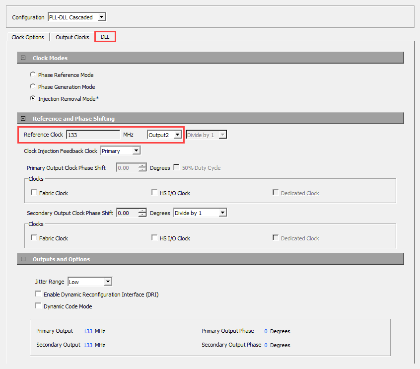
The following figure shows DLL configuration settings in Injection Removal Mode.
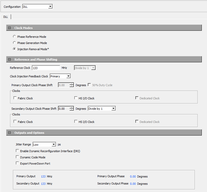
The following parameters are configurable in Injection Removal Mode:
Reference Clock frequency: Enter the reference clock frequency—ranges from 133 MHz–800 MHz.
Clock Injection Feedback Clock: Select the DLL feedback clock source between primary clock output and secondary clock output.
Primary Output Clock Options
- Phase Shift: This feature is not available in this mode.
- 50% Duty Cycle: This feature is not available in this mode.
- Select primary output clock connectivity
- Fabric Clock: Connects the primary output clock to the global clock network.
- HS I/O Clock: Connects the primary output clock to a high-speed I/O clock network.
- Dedicated Clock: This feature is not available in this mode.
Secondary Output Clock Options
- Phase Shift: This feature is not available in this mode.
- 50% Duty Cycle: This feature is not available in this mode.
- Clock Division: secondary clock output can be divided by 1, 2, or 4.
- Select secondary output clock connectivity:
- Fabric Clock: Connects the primary output clock to the global clock network.
- HS I/O Clock: Connects the primary output clock to a high-speed I/O clock network.
- Dedicated Clock: This feature is not available in this mode.
Outputs and Options
- Jitter Range: Select between Low, Medium Low, Medium High, and High.
- Select Enable Dynamic Reconfiguration Interface to expose the bus interface for DLL dynamic configuration.
- Select Export PowerDown Port to expose the port to the fabric.
The following figure shows DLL reference clock selection under PLL-DLL Cascaded configuration. Select PLL Output2 or Output3 as reference clock to the DLL. Enter the frequency for selected reference clock (PLL Output2 or Output3) under PLL Output Clocks tab. The rest of PLL and DLL settings must be configured as explained in the preceding configurator.