5.3 Zero-Crossing Configuration
The PL360 device has a dedicated digital input pin to be connected to a signal that provides a pulse derived from the mains Zero-Crossing (ZC). This pulse is generated by an external circuit connected to the mains. The PL360 PHY layer uses this pin to estimate the ZC time and period, implementing a PLL algorithm to reduce the effect of jitter in the pulse.
The G3-PLC PHY layer calculates the electrical phase difference between
transmitter and receiver for a given frame (uc_zct_diff in PHY-DATA.indication). To do so, both
devices have to be able to detect the ZC time of the mains.
The PRIME PHY layer does not calculate the electrical phase difference between transmitter and receiver, but it is possible to read the last mains Zero-Crossing time (ATPL360_REG_ZC_TIME (0x4006)) and period (ATPL360_REG_ZC_PERIOD (0x403B)) to calculate the phase difference in upper layers.
There are three parameters related to the ZC detection circuit used and the mains frequency. The default values of these parameters were calibrated with the reference hardware designs provided by Microchip and 50 Hz mains frequency. If a different ZC detection circuit is used or the mains frequency is different, these parameters must be configured accordingly:
- Mains frequency: It is the expected frequency of the mains signal. The PLL algorithm is able to adapt itself to a different mains frequency, but the closer the configured parameter is to the actual frequency, the faster the adaptation will be.
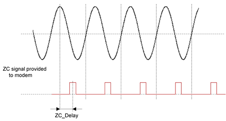
- ZC pulse delay: Due to hardware design reasons, the pulse generated by the ZC circuit may not be fully synchronized with the real mains ZC. The delay has to be measured between the highest point of the mains signal and the middle of the pulse provided to the PL360 device (see Figure 5-1).
- ZC pulse polarity: It indicates if the
pulse is positive, as in Figure 5-1, or
negative.
- G3-PLC: ATPL360_REG_ZC_CONF_INV (0x4037)
- PRIME: ATPL360_REG_ZC_CONF_INV (0x401A)