
9.9.5 Timing Path Example
The following procedure provides an example of working with timing paths.
- Make sure the design completed the Place and Route step successfully .
- Open SmartTime Maximum/Minimum Analysis View.
- Open Chip Planner.
-
In the SmartTime Maximum/Minimum Analysis View, right-click the net
CLK_ibuf/U0/U_IOPAD:PAD in the table and choose Show Path in Chip
Planner.
The net is selected (highlighted in red) in the Chip Canvas view and the three macros connected to the net are highlighted in white in the Chip Canvas view.Note: If Chip Planner is not open, Show Path in Chip Planner is gray and unavailable.
Figure 9-5. Cross-Probing – Timing Path 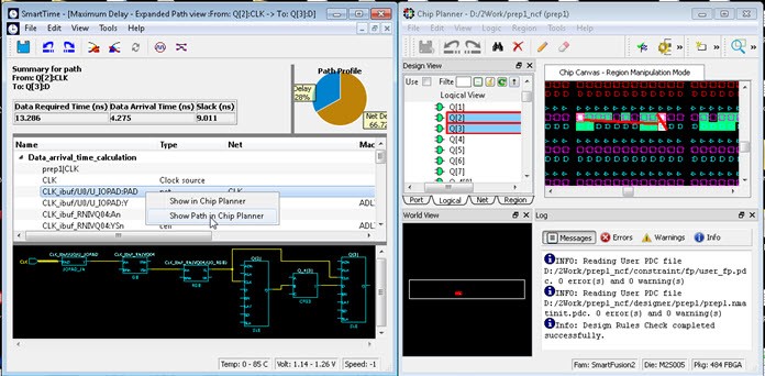
Figure 9-6. Cross-Probing Path from Max/Min Delay Analysis View Table 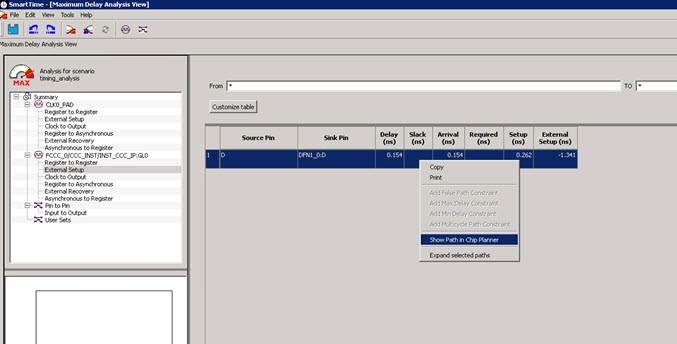
Instead of performing step 4, you can right-click a path in the Max/Min Delay Analysis View and choose Show Path in Chip Planner to cross-probe the path.