9.9.6 Port Example
- Make sure the design completed the Place and Route step successfully.
- Open SmartTime Maximum/Minimum Analysis View.
- Open Chip Planner.
-
In the SmartTime Maximum/Minimum Analysis View, right-click the Port “CLK” in
the Path and choose Show in Chip Planner.
The Port “CLK” is selected and highlighted in the Chip Planner Port View.Note: If Chip Planner is not open, Show in Chip Planner is gray and unavailable.
Figure 9-7. Cross-Probing – Port 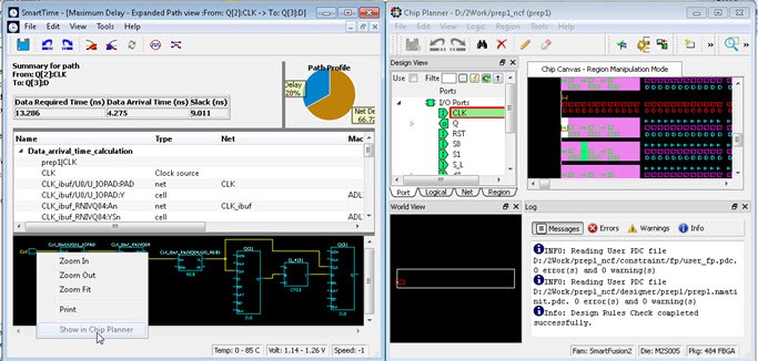
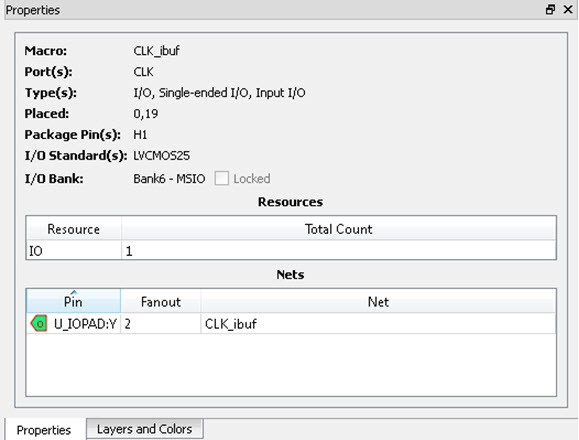
From the Properties View inside Chip Planner, you will find useful information about the Port “CLK” you are cross- probing:
- Port Type
- Port Placement Location (X-Y coordinates)
- I/O Bank Number
- I/O Standard
- Pin Assignment
Figure 9-8. Properties View of Port “CLK”