
3.2 PCIe Configurator
(Ask a Question)The PCIe configurator is used to build a PCIe endpoint or root port PCIe block. The configurator sets up the correct PCIESS registers and ports based on the user inputs.
To create a configured PCIe component, follow the steps:
- Access the PCIe module in the Features from the catalog, as shown in the following figure. Double click PCI Express; the Create Component dialog box is displayed.
Figure 3-2. PCIe Selection from Catalog 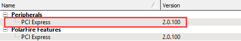
- Enter the name of the component and then click OK to launch the configurator, as shown in the following figure. The GUI allows you to select the related PCIe properties.
Figure 3-3. PCIe General Settings 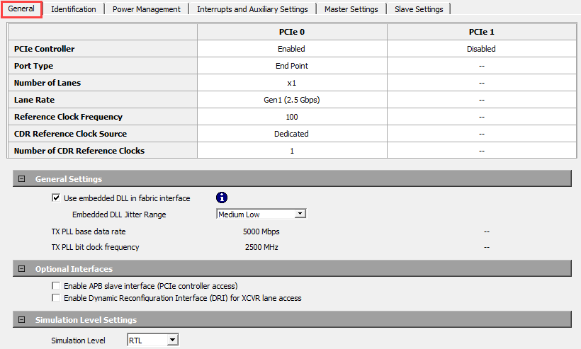
The following table lists the options available in the General tab.
| PCIE General Settings (PCIe 0 and PCIe 1) | Options | Default |
|---|---|---|
| PCIe Controller | Enabled and Disabled | PCIe 0 = Enabled PCIe 1 = Disabled |
| Port Type | End Point and Root Port1 | End Point |
| Number of Lanes | x1, x2, and x4 | x1 |
| Lane Rate | Gen1 (2.5 Gbps) and Gen2 (5.0 Gbps) | PCIe 0 = Enabled PCIe 1 = Disabled |
| Reference Clock Frequency (MHz) | 100, 125, and 156.25 | 100 |
| CDR Reference Clock Source | Dedicated and Fabric | Dedicated |
| Number of CDR Reference Clocks | 1 and 2 | 1 |
| Embedded DLL in fabric interface2 | Enabled and Disabled | Enabled |
| Embedded DLL Jitter Range | Low, Medium-Low, Medium-High, and High | Medium-Low |
| Optional Interfaces | ||
| APB Slave Interface3, 4 | Enabled and Disabled | Disabled |
| DRI Slave Interface5 | Enabled and Disabled | Disabled |
- The PCIe Slot Capabilities register of PolarFire SoC FPGA is a read-only register and the to Slot Power Limit and Slot Power Scale fields are hardwired to zeros. Hence, the PCIe Root Port advertises the Slot Power Limit as zero to the add-in card. However, the PCIe endpoints whose power requirement is 25W or below work as expected. For PCIe endpoints whose power requirement is more than 25W or needs a strict adherence to PCIe spec, it is recommended to connect the endpoint through a Microchip SwitchTec Gen3 PCIe Switch.
- AXI clock frequency must be greater than or equal to 125 MHz when the embedded DLL is enabled. Select the Use embedded DLL in the fabric interface option for removing clock insertion delay.
- APB interface is used to configure PCIe control registers.
- The PCIe APB_S_CLK supports a frequency range between 50 MHz to 125 MHz.
- For PolarFire SoC FPGA, DRI interface is used to configure lane related registers.
Number of Lanes: PCIe requires selection of the initial lane width. Wider lane-width cores are capable of training down to smaller lane widths if attached to smaller lane-width devices. The configurations, x2 and x4 support automatic lane reversal, allowing the PCIe link to permit board interconnections with reversed lane numbers, and the PCIESS continues to link train successfully and operate normally.
Reference Clock Frequency: PCIESS requires a 100 MHz, 125 MHz, or 156.25 MHz clock input. The specified clock frequency must match with the TXPLL clock frequency.
Optional Interfaces (APB Slave/DRI Slave): Enabling these options, exposes the particular bus on the PCIESS component for connecting to the FPGA fabric of the APB and DRI.
The following figure shows the options available in the Identification tab.
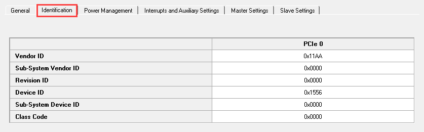
The following table lists the options available in the Identification tab.
| PCIE Identification Settings (PCIe 0 and PCIe 1) | Options | Default |
|---|---|---|
| Vendor ID | User Input | 0x11AA |
| Sub-System Vendor ID | User Programmable | 0x0000 |
| Revision ID | User Input | 0x0000 |
| Device ID | User Input | 0x1556 |
| Sub-System Device ID | User Input | 0x0000 |
| Class Code | User Input | 0x0000 |
Vendor ID: It identifies the manufacturer of the device or application. The default value (0x11AA) is the vendor ID of Microchip and is registered with PCI-Sig. Customized vendor identification IDs can also be used.
Sub-System Vendor ID: This ID further qualifies the manufacturer of the device or application. The default value is 0x0000 matching the vendor ID. Customized vendor identification IDs can also be used.
- 0x0000 is not recommended for vendor IDs or sub-system vendor ID.
- SSVID/SSDID value of 0x0000 causes the Endpoint to fail the PCIECV compliance tests when non-zero SSVID/SSDID is a requirement by the PCIe specification.
Revision ID: This indicates the revision of the device or application; an extension of the device ID. The default value is 0x0000. Customized revision IDs can also be used.
Device ID: A unique identifier for the application. This can be any value based on the input.
Sub-System Device ID: This is similar to sub-system vendor ID and further qualifies the device application.
Class Code: The class code identifies the general function of a device, and is divided into three byte-size fields:
- Base Class: Broadly identifies the type of the function performed by the device.
- Sub-Class: More specifically identifies the device function.
- Interface: Defines a specific register-level programming interface.
Class code encoding details can be found at www.pcisig.com.
The following figure shows the options available in the Power Management tab. Selecting the power management option allows loading settings to the PCIe config space headers.
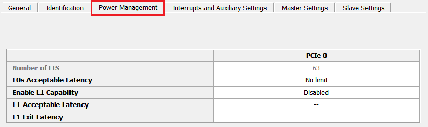
The following table lists the options available in the Power Management tab.
| PCIE Power Management Settings (PCIe 0 and PCIe 1) | Options | Default |
|---|---|---|
| Number of Fast Training Sequences (FTS) | — | 63 (Not configurable by the user) |
| L0 Standby (L0s) Acceptable Latency | No Limit Maximum of 64 ns Maximum of 128 ns Maximum of 256 ns Maximum of 512 ns Maximum of 1 µs Maximum of 2 µs Maximum of 4 µs | No Limit |
| Enable L1 Capability | Disabled and Enabled | Disabled |
| L1 Acceptable Latency | No Limit Maximum of 1 µs Maximum of 2 µs Maximum of 4 µs Maximum of 8 µs Maximum of 16 µs Maximum of 32 µs Maximum of 64 µs | No Limit |
| L1 Exit Latency | Less than 1 µs 1 µs less than 2 µs 2 µs less than 4 µs 4 µs less than 8 µs 8 µs less than 16 µs 16 µs less than 32 µs 32 µs to 64 µs more than 64 µs | 16 µs to less than 32 µs |
The PCIe base specification defines two levels of active state power management (ASPM) that are designed to provide options for trading off increased power conservation with rapid recovery to the L0 state.
Number of fast training sequences (FTS): The specific number to be repeated is defined by the receiving device and broadcast during training sequences at the link up time. The more FTS transmitted, the easier it is to obtain a receiver lock on the transmitted signal. By default, the number of FTS is grayed out, fixed to 63, and is not configurable by the user.
L0s Acceptable Latency: This state is required by all the PCIe devices and applies to a single direction on the link. The latency to return to L0 from L0s is specified to be very short. When entering L0s, the device moving into the power saving state sends an electrical idle ordered set (EIOS) to the receiving device, and then turn off the power to its transmitter. When returning from L0s to L0, the device must first generate a specific number of small order known as FTS. However, the purpose of L0s is to regain receiver lock and be able to receive traffic as quickly as possible, so the receiving device selects the lowest number of FTS that ensure clock recovery based on its specific design. This selection is used to choose a time interval to achieve L0s.
Enable L1 Compatibility: The L1 ASPM is optionally enabled and can be entered to achieve a greater degree of power conservation. In this state, both directions of the link are placed in the L1 state. Return to L0 requires both devices to go through the link recovery process which results in a greater latency to return to L0, so that the power state can typically be used when activity on the link is not expected for some significant time period.
L1 Acceptable Latency: To enter the L1 state, the downstream device must first request permission from the upstream device for entering in to a deeper power conservation state. Upon acknowledgement, both devices turn off their transmitters and enter an electrical idle state. This settings gives the allowable time to wait to achieve L1.
L1 Exit Latency: Returning from L1 requires, that both devices must now go through the link recovery process. The link recovery process uses TS1 and TS2 standard ordered sets as opposed to the smaller FTSs used by L0s. This setting selects the time interval to exit from L1.
The following figure shows the options available in the Interrupts and Auxiliary Settings tab.
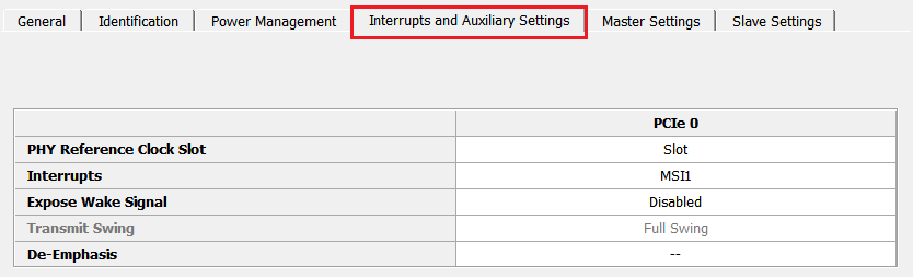
The following table lists the options available in the Interrupt and Auxiliary Settings tab.
| PCIE Interrupts and Auxiliary Settings (PCIe 0 and PCIe 1) | Options | Default |
|---|---|---|
| Physical layer reference clock slot | Slot and Independent | Slot |
| Interrupts | INTx, MSI 1, MSI 2, MSI 4, MSI 8, MSI 16, and MSI 32 | INTx |
| Expose wake signals1 | Enabled and Disabled | Enabled |
| Transmit swing | — | Full swing (Not configurable by the user) |
| De-Emphasis | −3.5 dB and −6 dB | −3.5 dB |
| (1) Enabled for End Point port type and disabled for Root Port by default. |
PHY Reference Clock Slot: Select this option, if the PHY reference clock is either from a PCIe slot or is generated separately. Slot is a clock source shared in the PCIe system between the host and endpoint link. An Independent slot is used in a system that uses the independent clock sources on either side of the link. This setting changes the PCIe configuration space register, to advertise the used clocked topology to the system root. It makes no other functional changes to the endpoint.
Interrupts: The PCIe EP implementation supports 32 MSI interrupt and INTx interrupts. It cannot simultaneously support both the interrupts. The PCIe EP supports legacy INT A interrupt as PolarFire is a single-function device.
Expose Wake Signals: Enabling this option, exposes the WAKE_N input signal on the PCIESS component allowing connection to the FPGA fabric.
De-Emphasis: This sets the de-emphasis (3.5 dB and 6.0 dB) for PCIe GEN 2 speed.
The following figure shows the options available in the Master Settings tab.
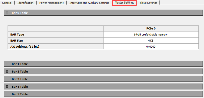
The following table lists the options available in the Master Settings tab.
| PCIE Master Settings (PCIe 0 and PCIe 1) | Options | Default |
|---|---|---|
| BAR Type | Disabled, 32-bit memory, 32-bit prefetchable memory, and 64-bit prefetchable memory | 32-bit memory |
| BAR Size | 4 KB, 8 KB, 16 KB, 32 KB, 64 KB, 128 KB, 256 KB, 512 KB, 1 MB, 2 MB, 4 MB, 8 MB, 16 MB, 32 MB, 64 MB, 128 MB, 256 MB, 512 MB,1 GB, 2 GB, and 4 GB | 4 KB |
| AXI Address [32 bit] | User Input, 32-bit address to be entered, lower 12 bits must be zero. | 0x0000 |
The following figure shows the options available in the Slave Settings tab.
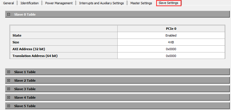
The following table lists the options available in the Slave Settings tab.
| PCIE Slave Settings (PCIe 0 and PCIe 1) | Options | Default |
|---|---|---|
| State | Disabled Enabled | Disabled |
| Size | 4 KB, 8 KB, 16 KB, 32 KB, 64 KB, 128 KB, 256 KB, 512 KB, 1 MB, 2 MB, 4 MB, 8 MB, 16 MB, 32 MB, 64 MB,128 MB, 256 MB, 512 MB, 1 GB, 2 GB, and 4 GB | 4 KB |
| AXI Address [32 bit] | User Input, 32-bit address to be entered, lower 12 bits must be zero. | 0x0000 |
| Translation Address [64 bit] | User Input, 64-bit address to be entered, lower 12 bits must be zero. | 0x0000 |
After making all selections in the PCIe configurator, complete the generation by clicking OK.
The next step is to create the XCVR_REFCLK and TX_PLL modules to be instantiated and connected to the PCIe block. Typically, the REF_CLK output of the PF_XCVR_REF_CLK is connected to the respective inputs of the PF_PCIE as well as the input REF_CLK of the PF_TX_PLL. For information on XCVR block generation, see PolarFire Family Transceiver User Guide.
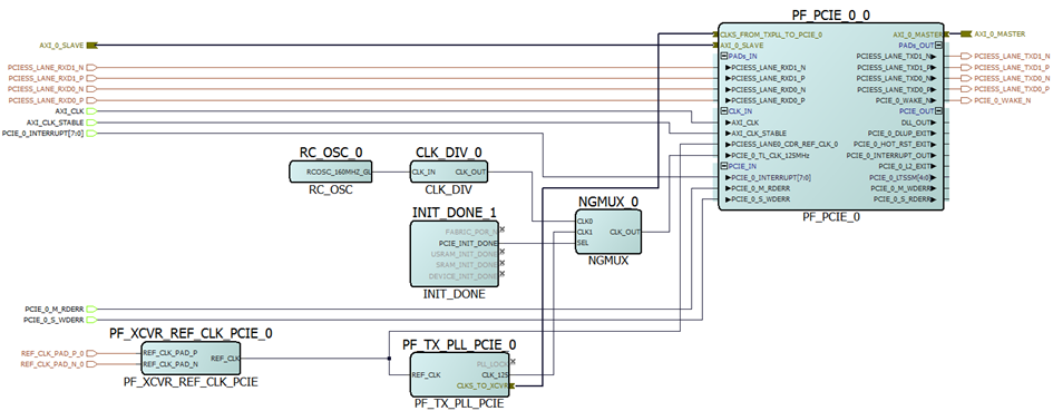
The following table lists the key connections of the SmartDesign PCIe example.
| Source | Destination |
|---|---|
| PF_XCVR_REF_CLK_PCIE_0:REF_CLK | PF_TX_PLL_PCIE_0:REFCLK |
| PF_PCIE_0_0:PCIESS_LANE0_CDR_REF_CLK_0 | |
| PF_TX_PLL_PCIE_0:CLKS_TO_XCVR | PF_PCIE_0_0:CLKS_FROM_TXPLL_TO_PCIE_0 |
| PF_TX_PLL_PCIE_0:CLK_125 | PF_PCIE_0_0:PCIE_0_TL_CLK_125MHz |