
3.4.8.1 mikroBUS1 Connector
The first mikroBUS™ socket (J79) implements all mikroBUS features, as shown in the schematic below. The reset feature is controlled (by default) by the PIO port PB21 and can be swapped with the system reset line or peripheral reset line by moving resistor R298 to R297 or R296, respectively.
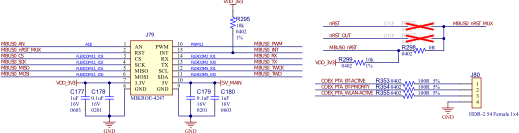
The first mikroBUS interface features an SPI bus shared with the second mikroBUS interface. Each interface has its own Chip Select line connected to its SPI interface (PB06 for the mikroBUS1 interface). PB4 (MISO) is shared between the two, which means that the SPI interface cannot be used at the same time on the two mikroBUS interfaces.
Both mikroBUS interfaces feature a two-wire interface (PA10 and PA11) that is also shared with the 40-pin RPi connector. The end user should ensure that the I²C addresses used on these nodes are different.
The PWM feature of the first mikroBUS interface (PD15) is shared with the second mikroBUS interface, which means that the PWM interface cannot be used at the same time on the two mikroBUS interfaces.
To evaluate the CAN FD interface, use specific mikroBUS Click boards™ featuring CAN FD transceivers rather than the standard UART RX/TX signals.
| Function | mikroBUS Signal | PIO | Pin No | Pin No | PIO | mikroBUS Signal | Function |
|---|---|---|---|---|---|---|---|
Analog input | MBUS0_AN | PC15 | 1 | 16 | PD15 | MBUS0_PWM | PWM |
Reset | MBUS0_nRST | PB21 | 2 | 15 | PC03 | MBUS0_INT | Interrupt |
SPI Chip Select | MBUS0_CS | PB06 | 3 | 14 | PA08 | MBUS0_RX | UART receive (mikroBUS output to SAM) |
SPI Clock | MBUS0_SCK | PB05 | 4 | 13 | PA07 | MBUS0_TX | UART transmit (mikroBUS input from SAM) |
SPI MISO | MBUS0_MISO | PB04 | 5 | 12 | PA11 | MBUS0_TWCK | TWI clock |
SPI MOSI | MBUS0_MOSI | PB03 | 6 | 11 | PA10 | MBUS0_TWD | TWI data |
VCC | VDD_3V3 | – | 7 | 10 | – | 5V_MAIN | VDD |
Ground | GND | – | 8 | 9 | – | GND | Ground |