
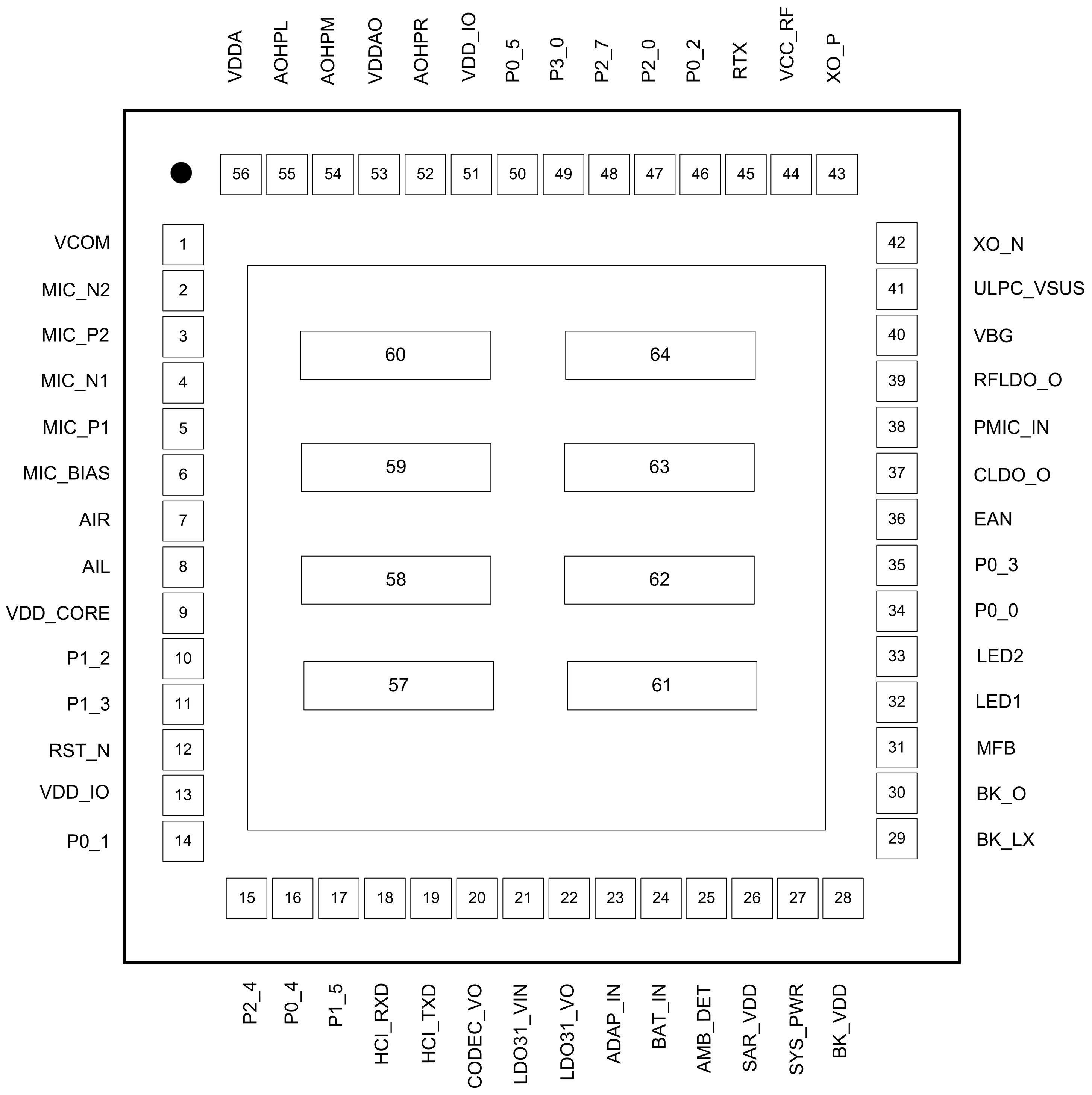
1.2 Pin Details
The following figure illustrates the pin diagram of the IS2062GM.
The following figure illustrates the pin diagram of the IS2064GM.

- IS2064GM-0L3 does not support an analog output from the DAC. The * on AOHPR, AOHPM, and AOHPL reflect the affected pins.
The following figure illustrates the pin diagram of the IS2064S.

The following figure illustrates the pin diagram of the IS2064B.

The following table provides the pin description of the IS2062GM, IS2064GM, IS2064S and IS2064B.
- I = Input pin
- O = Output pin
- I/O = Input/Output pin
- P = Power pin
| IS2062GM Pin No | IS2064GM-012 and IS2064S Pin No | IS2064GM-0L3 Pin No | IS2064B Ball No | Pin Type | Pin Name | Description |
|---|---|---|---|---|---|---|
| 53 | 1 | 1 | — | P | VDDAO | Power supply (3.0V to 3.6V) dedicated to codec output amplifiers; connect to CODEC_VO pin |
| 54 | 2 | — | A4 | O | AOHPM | Headphone common mode output/sense input |
| 55 | 3 | — | A3 | O | AOHPL | Left channel, analog headphone output |
| 56 | 4 | 4 | A2 | P | VDDA | Analog reference voltage. Do not connect, for internal use only |
| 1 | 5 | 5 | B3 | P | VCOM | Internal biasing voltage for codec, connect a 4.7 μF capacitor to ground |
| 4 | 6 | 6 | C1 | I | MIC_N1 | MIC1 mono differential analog negative input |
| 5 | 7 | 7 | D1 | I | MIC_P1 | MIC1 mono differential analog positive input |
| 2 | — | — | A1 | I | MIC_N2 | MIC2 mono differential analog negative input |
| 3 | — | — | B1 | I | MIC_P2 | MIC2 mono differential analog positive input |
| 6 | 8 | 8 | C2 | P | MIC_BIAS | Electric microphone biasing voltage |
| 7 | 9 | 9 | E1 | I | AIR | Right channel, single-ended analog input |
| 8 | 10 | 10 | F1 | I | AIL | Left channel, single-ended analog input |
| 9 | 11 | 11 | D2 | P | VDD_CORE | Core 1.2V power input; connect to CLDO_O pin; connect to GND through a 1 μF (X5R/X7R) capacitor |
| 10 | 12 | 12 | — | O | P1_2 | I2C SCL (Internal EEPROM clock), do not connect |
| 11 | 13 | 13 | E2 | I/O | P1_3 | I2C SDA (Internal EEPROM data) requires external 4.7 kOhm pull-up resistor |
| 12 | 14 | 14 | F2 | I | RST_N | System Reset (active-low) |
| 13 | 15 | 15 | B2 | P | VDD_IO | I/O power supply input (3.0V to 3.6V); connect to LDO31_VO; connect to GND through a 1 μF (X5R/X7R) capacitor |
| 14 | 16 | 16 | G1 | I/O | P0_1 | Configurable control or indication pin
(Internally pulled up, if configured as an input)
|
| 15 | 17 | 17 | G2 | I/O | P2_4 | For IS2062GM/64GM (Flash variant): External address bus negative, System configuration pin along with the P2_0 and EAN pins can be used to set the SoC in any one of the following three modes:
For IS2064S/B (ROM variant): Do not connect this pin |
| 16 | 18 | 18 | H2 | I/O | P0_4 | Configurable control or indication pin
(Internally pulled-up, if configured as an input)
|
| 17 | 19 | 19 | H3 | I | P1_5 | Configurable control or indication pin
(Internally pulled-up, if configured as an input)
|
| 18 | 20 | 20 | H4 | I | HCI_RXD | HCI UART data input |
| 19 | 21 | 21 | H5 | O | HCI_TXD | HCI UART data output |
| 20 | 22 | 22 | H1 | P | CODEC_VO | LDO output for codec power |
| 21 | 23 | 23 | J1 | P | LDO31_VIN | LDO input, connect to SYS_PWR |
| 22 | 24 | 24 | J2 | I | LDO31_VO | 3V LDO output for VDD_IO power, do not calibrate |
| 23 | 25 | 25 | J3 | P | ADAP_IN | 5V power adapter input, used to charge the battery in case of Li-Ion battery power applications |
| 24 | 26 | 26 | J4 | P | BAT_IN |
Power Supply input. Voltage range: 3.2V to 4.2V. Source can either be a Li-Ion battery or any other power rail on the host board |
| 25 | 27 | 27 | H6 | P | AMB_DET | Analog input for ambient temperature detection |
| 26 | 28 | 28 | J5 | P | SAR_VDD | SAR 1.8V input; connect to BK_O pin |
| 27 | 29 | 29 | J6 | P | SYS_PWR | System power output derived from the ADAP_IN or BAT_IN. Do not connect, for internal use only |
| 28 | 30 | 30 | J7 | I | BK_VDD | 1.8V buck VDD power input; connect to SYS_PWR pin |
| 29 | 31 | 31 | J8 | I | BK_LX | 1.8V buck regulator feedback path |
| 30 | 32 | 32 | J9 | I | BK_O | 1.8V buck regulator output. Do not connect to other devices. For internal use only |
| 31 | 33 | 33 | H9 | P | MFB |
|
| — | 34 | 34 | — | P | LED3 | LED driver 3 |
| 33 | 35 | 35 | G9 | P | LED2 | LED driver 2 |
| 32 | 36 | 36 | F9 | P | LED1 | LED driver 1 |
| — | 37 | 37 | — | P | P3_7 | Configurable control or indication pin
(Internally pulled-up, if configured as an input)
|
| — | 38 | 38 | — | P | P3_5 |
Configurable control or indication pin (Internally pulled-up, if configured as an input) |
| 34 | 39 | 39 | H7 | I/O | P0_0 | Configurable control or indication pin
(Internally pulled-up, if configured as an input)
|
| 35 | 40 | 40 | H8 | I/O | P0_3 | Configurable control or indication pin
(Internally pulled-up, if configured as an input)
|
| 36 | 41 | 41 | — | I/O | EAN | For IS2062GM/64GM (Flash variant): External address-bus negative System configuration pin along with the P2_0 and P2_4 pins can be used to set the SoC in any one of the following three modes:
For IS2064S/B (ROM variant): Do not connect for this pin |
| — | 42 | 42 | — | P | AVDD_USB | USB power input; connect to LDO31_VO pin |
| — | 43 | 43 | — | I/O | DM | Differential data-minus USB |
| — | 44 | 44 | — | I/O | DP | Differential data-plus USB |
| 37 | 45 | 45 | E9 | P | CLDO_O | 1.2V core LDO output for internal use only. Connect to GND through a 1 μF capacitor |
| 38 | 46 | 46 | D9 | P | PMIC_IN | 1.8V power input for internal blocks; connect to BK_O |
| 39 | 47 | 47 | C9 | P | RFLDO_O | 1.28V RF LDO output for internal use only. Connect to GND through a 1 μF capacitor |
| 40 | 48 | 48 | D8 | P | VBG | Bandgap output reference for decoupling interference, connect to GND through a 1 μF capacitor |
| 41 | 49 | 49 | C8 | P | ULPC_VSUS | ULPC 1.2V output power, maximum loading 1 mA, connect to GND through a 1 μF capacitor |
| 42 | 50 | 50 | B9 | I | XO_N | 16 MHz crystal input negative |
| 43 | 51 | 51 | A9 | I | XO_P | 16 MHz crystal input positive |
| 44 | 52 | 52 | A8 | P | VCC_RF | RF power input (1.28V) for both synthesizer and Tx/Rx block, connect to RFLDO_O |
| 45 | 53 | 53 | A7 | I/O | RTX/ RF_RTX | RF path (transmit/receive) |
| — | 54 | 54 | — | I/O | P3_1 | Configurable control or indication pin
(Internally pulled-up, if configured as an input)
|
| — | 55 | 55 | — | I/O | P3_3 | Configurable control or indication pin
(Internally pulled-up, if configured as an input)
|
| — | 56 | 56 | — | I/O | P3_6 | Configurable control or indication pin
(Internally pulled-up, if configured as an input)
|
| 46 | 57 | 57 | G8 | I/O | P0_2 | Configurable control or indication pin
(Internally pulled-up, if configured as an input)
|
| 47 | 58 | 58 | D5 | I/O | P2_0 | For IS2062GM/64GM (Flash variant): External address-bus negative System configuration pin along with the P2_4 and EAN pins can be used to set the SoC in any one of the following three modes:
For IS2064S/B (ROM variant): Do not connect for this pin |
| 48 | 59 | 59 | F8 | I/O | P2_7 | Configurable control or indication pin
(Internally pulled-up, if configured as an input)
|
| 49 | 60 | 60 | E8 | I/O | P3_0 | Configurable control or indication pin
(Internally pulled-up, if configured as an input)
|
| — | 61 | 61 | — | I/O | TFS0 | I2S interface: left/right clock |
| 50 | 62 | 62 | B8 | I/O | P0_5 | Configurable control or indication pin
(Internally pulled-up, if configured as an input)
|
| 51 | 63 | 63 | B2 | P | VDD_IO | I/O power supply input (3V to 3.6V); connect to LDO31_VO pin, connect to GND through a 1 μF (X5R/X7R) capacitor |
| — | 64 | 64 | B7 | I/O | DR0 | I2S interface: digital left/right data |
| — | 65 | 65 | B6 | I/O | RFS0 | I2S interface: left/right clock |
| — | 66 | 66 | B5 | I/O | SCLK0 | I2S interface: bit clock |
| — | 67 | 67 | B4 | I/O | DT0 | I2S interface: digital left/right data |
| 52 | 68 | — | A5 | O | AOHPR | Right-channel, analog headphone output |
| 57-64 | 69-83 | 69-83 | — | P | EP | Exposed pads, Used as ground (GND) pins |
| — | — | — | A6, E4, E5, E6, F5 | P | GND | Ground reference |