
1.1 FlashROM
FlashROM memory provides the security of stored data in addition to a 128-bit AES decryption core. You can read, modify, and write to the FlashROM using the JTAG interface; however, you can only read it from the FPGA core.
FlashROM memory provides the security of stored data in addition to a 128-bit AES decryption core. You can read, modify, and write to the FlashROM using the JTAG interface; however, you can only read it from the FPGA core.
FlashROM is available from within the Libero® IDE Project Manager or the SmartGen tool in standalone Designer. Add a FlashROM core from the catalog to your SmartDesign in the Libero IDE Project Manager, or start SmartGen and select the FlashROM from the catalog.
Adding a FlashROM core opens a special FlashROM core generator that enables you to configure the FlashROM functionality.
IGLOO® and ProASIC® 3 devices have a flexible programming option. The FlashROM and the FPGA core fabric can be programmed independently of each other, allowing the FlashROM to be updated without changing the FPGA core fabric. The following are just a few examples of possible applications for the FlashROM feature:
- Internet protocol (IP) addressing (wireless or fixed)
- System-calibration settings
- Device serialization and/or inventory control
- Subscription-based business models (for example, set-top boxes)
- Secure key storage
- Asset management tracking
- Date stamping
- Version management
The FlashROM is programmed using the standard IEEE1532 JTAG programming interface. Pages can be individually programmed (erased and written), and on-chip AES decryption can be used selectively to load data securely into the FlashROM (such as application-based security keys stored in the FlashROM for a design). For information on how to program your FlashROM-enabled devices, see the FlashPoint User Guide.
The FlashROM can selectively be read back either through the JTAG programming interface or via direct FPGA core addressing. Its contents can only be updated via the JTAG interface. A seven-bit address from the FPGA core defines which of the eight pages (3 MSBs of the address) is being read and which of the 16 bytes in the page (4 LSBs) are being read.
The FlashROM is physically organized as 8x128 bit blocks and logically organized as eight pages by 16 bytes. Only Flash FPGAs contain on-chip nonvolatile memory (NVM); IGLOO, Fusion, and ProASIC3 devices are the only FPGAs to support this feature.
You can assign specific regions of the FlashROM for specific purposes by floorplanning the FlashROM and assigning properties. The content of these regions can be modified during programming time if you assign a modifiable content property to a given region. If you do not want the FlashROM content to be modified, you can fix the content in SmartGen.
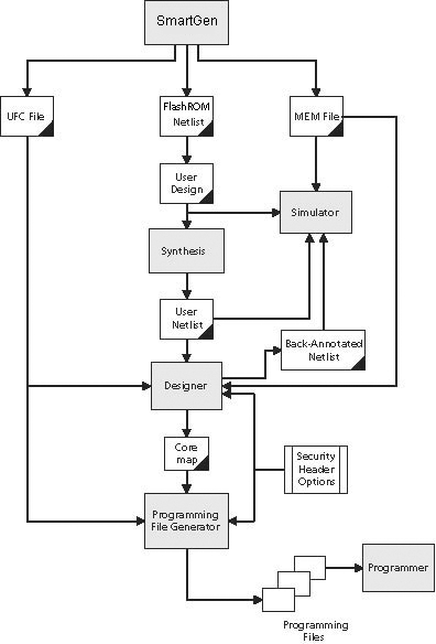
When you generate a new FlashROM file, the generator saves the following files for you to use throughout the design cycle:
- CXF file - Contains project info for Libero IDE.
- Netlist file - use this file to instantiate your core, just as you would instantiate any other core in your design
- UFC file - User Flash configuration file; it contains all the configuration information regarding the FlashROM data content and is used for programming. You can export a core map file that contains the core programming information and use it along with the UFC file to generate programming files. Designer software supports importing the UFC file and launching the programming file generator to merge the FPGA core map file and the FlashROM programming file.
- MEM file - FlashROM specific memory initialization file. The MEM file has 128 rows of eight bits, representing the contents of the FlashROM. FlashROM defaults to 0s for any unspecified locations of the FlashROM memory. This file is used exclusively for simulation.
- Configure FlashROM
- Simulate Pre/Post Synthesis
- Synthesize
- Place-and-Route
- Run Back-Annotation and Timing Simulation
- Specify security settings
- Specify FlashROM content
- Generate a programming file