
2.1.3.2.2 Two-Port LSRAM Configurator
(Ask a Question)The Two-Port SRAM (TPSRAM) IP configurator is available in the Libero SoC software under Memory & Controllers. The following figure shows the TPSRAM IP block available in the Libero SoC software. The TPSRAM configurator enables write access on one port and read access on the other port. The RAM configurator automatically cascades LSRAM blocks to create wider and deeper memories by selecting the most efficient aspect ratio. It also handles the grounding of unused bits. The core configurator supports the generation of memories that have different write and read aspect ratios. The configurator uses one or more memory blocks to generate a RAM matching the configuration. In addition, it also creates the surrounding cascading logic.
The configurator cascades RAM blocks in three different methods:
- Cascaded deep—For example, two blocks of 16384 x 1 combined to create a 32768 x 1.
- Cascaded wide—For example, two blocks of 16384 x 1 combined to create a 16384 x 2.
- Cascaded wide and deep—For example, four blocks of 16384 x 1 combined to create a 32768 x 2, in two blocks width-wise by two blocks depth-wise configuration.
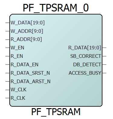
| Port | Direction | Polarity | Description |
|---|---|---|---|
| CLK | Input | Rising edge | Single clock to drive both W_CLK and R_CLK. Applicable only when single read/write clock is selected. |
| W_DATA[19:0] | Input | — | Write data |
| W_ADDR[9:0] | Input | — | Write address |
| W_EN | Input | Active High | Write port enable |
| W_CLK | Input | Rising edge | Write clock. Applicable only when independent clocks are selected. |
| R_CLK | Input | Rising edge | Read clock. Applicable only when independent clocks are selected. |
| R_EN | Input | Active High | Read data enable. |
| WBYTE_EN[] | Input | — | Write enable for byte write. |
| R_ADDR[9:0] | Input | — | Read address |
| R_DATA[19:0] | Output | — | Read data |
| R_DATA_EN | Input | Active High | Read data register enable |
| R_DATA_SRST_N | Input | Active Low | Read data register synchronous reset |
| R_DATA_ARST_N | Input | Active Low | Read data register asynchronous reset |
| SB_CORRECT | Output | Active High | Single-bit correct flag. Applicable only when ECC is enabled. |
| DB_DETECT | Output | Active High | Double-bit detect flag. Applicable only when ECC is enabled. |
| ACCESS_BUSY | Output | Active High | Busy signal from SmartDebug. Exposed only when Expose ACCESS_BUSY output is checked. |
- Parameter settings
- Port settings
- Memory initialization settings
Parameter Settings
The parameter settings include the Optimization for High Speed or Low Power, clock signals settings, and optional port settings. The following figure shows the TPSRAM block configurator.

Optimization for High Speed or Low Power
- High Speed—Optimizes the LSRAM macro for speed and area by using width cascading.
- Low Power—Optimizes the LSRAM macro for low power, but it uses additional logic at the input and output by using depth cascading.
Single Read/Write Clock (CLK) or Independent Read/Write Clocks
- Single clock—Drives write and read with the same clock. This is the default configuration for Two-Port LSRAM.
- Independent clocks—Selects independent clock for Read (R_CLK) and Write (W_CLK)—R_CLK and W_CLK.
- Rising edge or Falling edge—Sets the signal polarity.
Optional Ports
- Lock access to SmartDebug—When enabled, SmartDebug access to the RAM is disabled.
- Expose ACCESS_BUSY output—When enabled, SmartDebug ACCESS_BUSY signal is available as top-level port.
Port Settings
In the Port Settings tab, the user can set RAM size, select ports, and set data output on write settings for both ports. The following figure shows the TPSRAM block port settings.
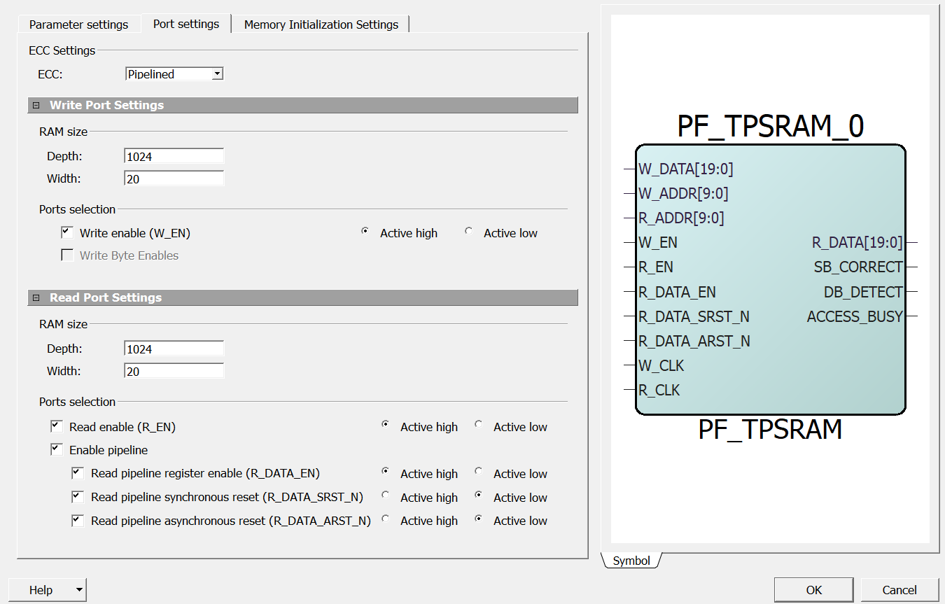
ECC
- Disabled
- Pipelined
- Non-pipelined
Write Byte Enable Settings
Write Byte Enables—Enables the writing of individual bytes of data (WBYTE_EN). This port is disabled while the ECC is enabled.
The Write Byte Enable bits are all the control signals exposed by each column of LSRAM blocks when the implementation splits the word width. The LSRAM configurator generates the most efficient configuration of the depth and width for high-speed or low-power selection. Depending on the generated configuration, each Write Byte Enable bit may control up to 10 bits of data. In other words, the Write Byte Enable option does not govern the implementation.
In low-power mode for word widths that are multiples of 8, each Write Byte Enable bit will control 8 bits unless the word width is also a multiple of 10. For example, generating a 32-bit word width LSRAM, with Write Byte Enables, will cascade the RAMs width-wise such that there are a total of 4 Write Byte Enable bits (2 per RAM block) and each Write Byte Enable bit controls the writing of 8-bits of data.
- Width of 17, is divided as 9 + 8.
- Width of 35, is first divided as 18 + 17, and then, divided as 9 + 9 + 9 + 8.
RAM Size
- Depth—Sets the depth range. The depth range for each port is between 1 and 524288. The maximum value depends on the die.
- Width—Sets the width range. The width range for each port is between 1 and 38080.
Write Enable (W_EN)—The default configuration for W_EN is checked (enabled). Clearing the W_EN option ties the signal to the Active state and removes it from the generated macro. Use Active high or Active low to change the signal polarity.
Read Enable (R_EN)—The default configuration for R_EN is unchecked (disabled), which ties the signal to the Active state and removes it from the generated macro. Selecting the check box enables R_EN and the associated functionality. Use Active high or Active low to change the signal polarity.
Enable Pipeline
- Read Pipeline Register Enable (R_DATA_EN)—The pipeline registers for R_DATA have an active high, enable input. By default, the check box is disabled. Selecting this check box adds the signal to the top-level port.
- Read Pipeline Synchronous Reset (R_DATA_SRST_N)—The pipeline registers for R_DATA have an active-low, synchronous reset input. By default, the check box is disabled. Selecting this check box adds the signal to the top-level port.
- Read Pipeline Asynchronous Reset (R_DATA_ARST_N)—The pipeline registers for R_DATA have an active-low, asynchronous reset input. By default, the check box is disabled. Selecting this check box adds the signal to the top-level port.
- Active high or Active low—sets the signal polarity.
Memory Initialization at Power-Up
In the Memory Initialization tab, the user can initialize RAM at power-up. LSRAM can be initialized during device power-up and functional simulation as described in Memory Initialization at Power-Up of Dual-Port Large SRAM Configurator. The following figure shows the TPSRAM IP memory initialization.
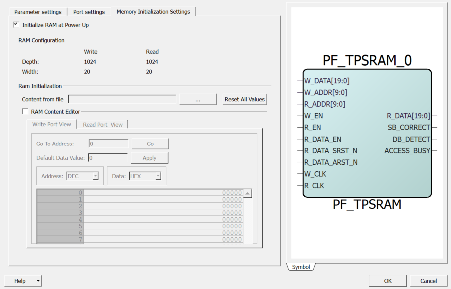
The Reset All Values option resets all the data values. This option is enabled when the RAM Content Editor check box is selected.