
2.1.3.2.1 Dual-Port Large SRAM Configurator
(Ask a Question)The PF_DPSRAM configurator is available in the .
The PF_DPSRAM configurator automatically cascades LSRAM blocks to create wider and deeper memories by selecting the most efficient aspect ratio. It also handles the grounding of unused bits. The configurator supports the generation of memories that have different aspect ratios on each port. The configurator uses one or more memory blocks to generate a RAM to match the configuration. The configurator also creates an external logic required for the cascading.
The configurator cascades RAM blocks in three different methods:
- Cascaded deep—For example, two blocks of 16384 x 1 are combined to create a 32768 x 1.
- Cascaded wide—For example, two blocks of 16384 x 1 are combined to create a 16384 x 2.
- Cascaded wide and deep—For example, four blocks of 16384 x 1 are combined to create a 32768 x 2, in a two-block width by two-block depth configuration.
For more information on Dual-Port mode, see Dual-Port Mode.
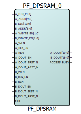
| Port | Direction | Polarity | Description |
|---|---|---|---|
| CLK | Input | Rising edge | Single-clock signal that drives both ports with the same clock. Exposed only when single clock is selected. |
| A_DIN[19:0] | Input | — | Port A write data |
| A_ADDR[9:0] | Input | — | Port A read address |
| A_BLK_EN | Input | Active High | Port A block select |
| A_CLK | Input | Rising edge | Port A clock. Applicable only when independent clocks are selected. |
| A_WEN | Input | — | Port A signal to switch between write and
read modes:
|
| A_REN | Input | — | Port A read data enable |
| A_WBYTE_EN[1:0] | Input | — | Port A write byte enable |
| A_DOUT[19:0] | Output | — | Port A read data |
| A_DOUT_EN | Input | Active High | Port A read data register enable |
| A_DOUT_SRST_N | Input | Active Low | Port A read data register synchronous reset |
| A_DOUT_ARST_N | Input | Active Low | Port A read data register asynchronous reset |
| B_DIN[19:0] | Input | — | Port B write data |
| B_ADDR[9:0] | Input | — | Port B address |
| B_BLK_EN | Input | Active High | Port B enable |
| B_CLK | Input | Rising edge | Port B clock. Applicable only when independent clocks are selected |
| B_WEN | Input | — | Port signal to switch between write and read
modes:
|
| B_REN | Input | — | Port B read data enable |
| B_WBYTE_EN[1:0] | Input | — | Port B write byte enable |
| B_DOUT[19:0] | Output | — | Port B read data |
| B_DOUT_EN | Input | Active High | Port B read data register enable |
| B_DOUT_SRST_N | Input | Active Low | Port B read data register synchronous reset |
| B_DOUT_ARST_N | Input | Active Low | Port B read data register asynchronous reset |
| ACCESS_BUSY | Output | Active High | Busy signal when being initialized or accessed using SmartDebug |
The dual-port LSRAM configurator has three tabs:
- Parameter settings
- Port settings
- Memory initialization
Parameter Settings
The parameter settings include the optimization of LSRAM for High Speed or Low Power, clock signal settings, and optional port settings. The following figure shows the Dual-Port Large LSRAM block configurator.
Optimization for High Speed or Low Power
- High Speed—Optimizes the LSRAM for speed and area by using width cascading.
- Low Power—Optimizes the LSRAM for low power by using depth cascading, it uses additional logic at the input and output.
Single Clock (CLK) or Independent Clocks (A_CLK and B_CLK)
- Single clock—Drives both A and B ports with the same clock. This is the default configuration for dual-port LSRAM.
- Independent clocks—Selects independent clock for each A_CLK for Port A and B_CLK for Port B).
- Rising edge or Falling edge—Changes the signal polarity.
Optional Ports
- Lock access to SmartDebug—When enabled, SmartDebug access to the RAM is disabled.
- Expose ACCESS_BUSY output—When enabled, SmartDebug ACCESS_BUSY signal is available as top-level port.
Port Settings
In the Port Settings tab, you can set the RAM size, select ports, and set data output on write settings for both Ports A and B. The following figure shows the PF_DPSRAM block port settings.
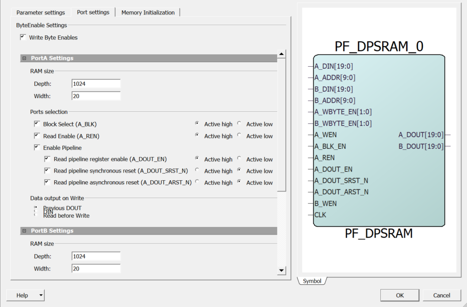
Byte Enable Settings
Write Byte Enables—Enables writing to individual bytes of data (A_WBYTE_EN and B_WBYTE_EN).
The Write Byte Enable bits are all the control signals exposed by each column of LSRAM blocks when the implementation splits the word width. The LSRAM configurator generates the most efficient configuration of the depth and width for high-speed or low-power selection. Depending on the generated configuration, each Write Byte Enable bit may control up to 10 bits of data. In other words, the Write Byte Enable option does not govern the implementation.
In low-power mode for word widths that are multiples of 8, each Write Byte Enable bit controls 8 bits unless the word width is also a multiple of 10. For example, generating a 32-bit word width LSRAM, with Write Byte Enables, cascades the RAMs width-wise such that there are a total of 4 Write Byte Enable bits (2 per RAM block) and each Write Byte Enable bit controls the writing of 8-bits of data.
- Width of 17, is divided as 9 + 8.
- Width of 35, is first divided as 18 + 17, and then, divided as 9 + 9 + 9 + 8.
RAM Size
- Depth—Sets the depth range. The depth range for each port is between 1 and 524288. The maximum value depends on the die.
- Width—Sets the width range. The width range for each port is between 1 and 19040.
Ports Selection: Block Select (A_BLK_EN and B_BLK_EN)
The default configuration for A_BLK_EN and B_BLK_EN is unchecked, which ties the signal to the Active state and removes it from the generated component. Select Active high or Active low to change the signal polarity. Ports are populated on the component by checking the respective check boxes.
Read Enable (A_REN and B_REN)
The default configuration for A_REN or B_REN is unchecked, which ties the signal to the active state and removes it from the generated macro. Select Active high or Active low to change the signal polarity. Ports are populated on the component by checking the respective check boxes.
Enable Pipeline
- Register Enable (A_DOUT_EN and B_DOUT_EN)—the pipeline registers for ports A and B have active-high, enable inputs. By default, the check box is disabled. Selecting this check box adds the signal to the top-level port.
- Synchronous Reset (A_DOUT_SRST_N and B_DOUT_SRST_N)—the pipeline registers for ports A and B have active-low, synchronous reset inputs. By default, the check box is disabled. Selecting this check box adds the signal to the top-level port.
- Asynchronous Reset (A_DOUT_ARST_N and B_DOUT_ARST_N)—the pipeline registers for ports A and B have active-low, asynchronous reset inputs. By default, the check box is disabled. Selecting this check box adds the signal to the top-level port.
Select Active high or Active low to change the signal polarity. Ports are populated on the component by checking their respective check boxes.
Data Output on Write
- Previous DOUT—The default data on the Read data output (A_DOUT or B_DOUT) during a write cycle is the DOUT data from the previous cycle (Previous DOUT).
- DIN—To enable feed-through write mode on Read data output.
- Read before Write—To perform a read operation before a write operation overwriting the previous data.
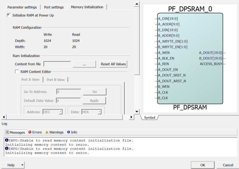
Memory Initialization at Power-Up
In the Memory Initialization tab, you can initialize RAM at power-up. LSRAM can be initialized during device power-up and functional simulation. The following figure shows the PF Dual Port Large SRAM IP memory initialization.
Initialize RAM at Power Up
- Initialize RAM at Power Up—Loads the RAM content during device operation at power-up and functional simulation.
- RAM Configuration—Both write and read depths and widths are displayed as specified in the Port settings tab.
- Initialize RAM Contents From File—The RAM’s content can be initialized by importing the memory file. This avoids the simulation cycles required for initializing the memory and reduces the simulation runtime. The configurator partitions the memory file appropriately so that the right content goes to the right block RAM when multiple blocks are cascaded.
- Import File—Selects and imports a memory
content file (Intel-Hex) from the Import Memory Content dialog box. File
extensions are set to
*.hexfor Intel-Hex files during import. For more information, see Appendix: Supported Memory File Formats for LSRAM and μSRAM. The imported memory content is displayed in the RAM Content Editor. - Reset All Values—Resets all the data values. This option is enabled when the RAM Content Editor check box is selected.
RAM Content Editor
The RAM Content Editor enables the user to specify the contents of RAM memory manually for both Port A and Port B. It also allows you to modify imported data.
- Go To Address—Enables you to go to a specific address in the editor. You can select the number display format (HEX, BIN, and DEC) from the Address menu.
- Default Data Value—You can set this with new data to change the default. When the data value is changed, all default values in the manager are updated to match the new value. You can select the number display format (HEX, BIN, and DEC) from the Data menu.
- Address—The Address column lists the address of a memory location. The menu specifies the number format of the address list (hexadecimal, binary, or decimal).
- Data—Controls the data format and data values in the manager.
Click OK to close the manager and save all changes made to the memory and its contents. Click Cancel to close the manager and cancel all the changes.