
20.2.2.3.9 Memory Partition and Protection
(Ask a Question)The Physical Memory Protection (PMP) prevents a process (running on a RISC-V Processor) or an initiator (FPGA Fabric) from accessing memory that has not been allocated to it. RISC-V system has PMP unit, which provides control registers for each processor to allow physical memory access privileges (read, write, execute) to be specified for each physical memory region. Similarly, the AXI Switch has Memory Protection Unit (MPU) block which provides register control to setup memory access regions for FPGA initiators.
DDR Memory Partition
The DDR Memory Partition tab allows the DDR memory to be allocated to cached and non-cached regions depending on the amount of DDR memory physically connected.

- The Offset Address (Base Address) for both cached and non-cached regions is fixed.
- High Address is the End Address based on the size.
- Users are expected to enter the
Range. Based on the Range selection, High Address and Physical DDR Offset is updated.
- When Range is set to zero, memory is not allocated in DDR.
- When Range is set to a nonzero value, it must be a multiple of 16 MB.
- Physical DDR Offset is allocation
of DDR memory (connected to the FPGA system) based on the nonzero Range
value.Important: When Setup Physical DDR Address manually option is enabled, the default Physical DDR Offset Address is set as 0x0000_0000 for all the regions and it is up to the user to change this address (when the size of the allocated memory region is greater than 0 bytes). When the size of allocated memory region is zero bytes, the offset and high address are reported as N/A and remains as a read-only field.
- Range is allocated sequentially
starting with 0x0000_0000 in the following order:
- Cached 32-bit
- Cached 64-bit
- Non-Cached 32-bit
- Non-Cached 64-bit
The following figure shows the graphical representation of how the Physical DDR Offset allocation is done based on the preceding ranges:
Figure 20-44. Physical DDR Offset — Graphical Representation 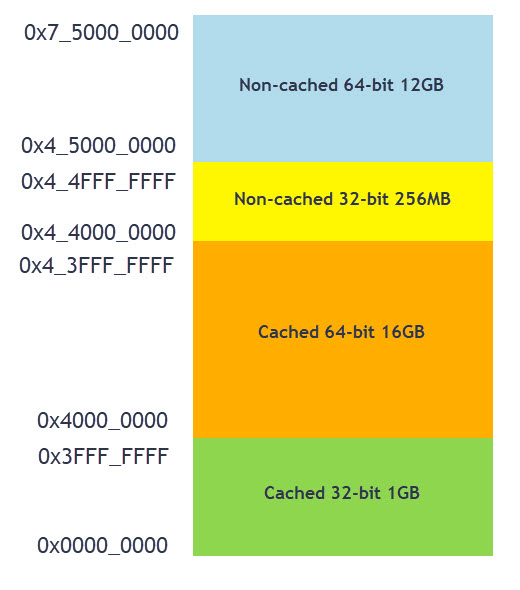
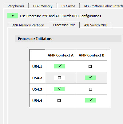
Processor PMP
The following figure shows the Processor PMP tab.

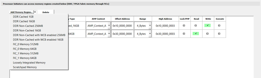
| Memory Type | Memory Size | Address Size | Address Range |
|---|---|---|---|
| DDR Cached | 512 MB | 32-bit | 0x80000000 - 0xBFFFFFFF |
| 16 GB | 64-bit | 0x10_00000000 - 0x13_FFFFFFFF | |
| DDR Non-Cached | 256 MB |
32-bit |
0xC0000000 - 0xCFFFFFFF |
| 16 GB | 64-bit | 0x14_00000000 - 0x17_FFFFFFFF | |
| DDR Non-Cached with WCB enabled | 256 MB | 32-bit | 0xC0000000 - 0xCFFFFFFF |
| 16 GB | 64-bit | 0x14_00000000 - 0x17_FFFFFFFF | |
| FIC_0 Memory | 512 MB | 32-bit | 0x60000000 - 0x7FFFFFFF |
| 64 GB | 64-bit | 0x20_00000000 - 0x2F_FFFFFFFF | |
| FIC_1 Memory | 512 MB | 32-bit | 0xE0000000 - 0xFFFFFFFF |
| 64 GB | 64-bit | 0x30_00000000 - 0x3F_FFFFFFFF | |
| Loosely Integrated Memory | — | — | Start Address is 0x0800_0000 |
| Scratch | — | — | Start Address is 0x0A00_0000 |
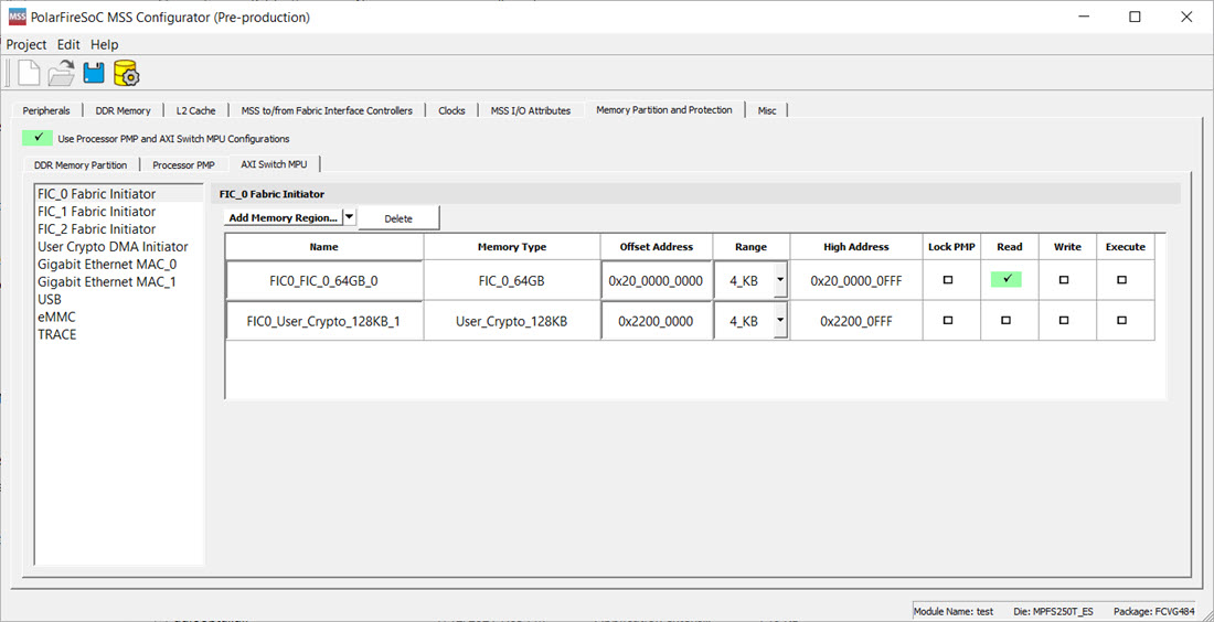
AXI Switch MPU
Memory Type | Memory Size | Address Size | Address Range |
|---|---|---|---|
| DDR Non-Cached | 256 MB | 32-bit | 0xC0000000 - 0xCFFFFFFF |
16 GB | 64-bit | 0x14_00000000 - 0x17_FFFFFFFF | |
FIC_0 Memory | 512 MB | 32-bit | 0x60000000 - 0x7FFFFFFF |
64 GB | 64-bit | 0x20_00000000 - 0x2F_FFFFFFFF | |
| FIC_1 Memory | 512 MB | 32-bit | 0xE0000000 - 0xFFFFFFFF |
64 GB | 64-bit | 0x30_00000000 - 0x3F_FFFFFFFF | |
FIC_3 Memory | 512 MB | 32-bit | 0x40000000 - 0x5FFFFFFF |
User Crypto Memory | 128 KB | 32-bit | 0x22000000 - 0x2201FFFF |