3.4.6.1 SDMMC1 Connector
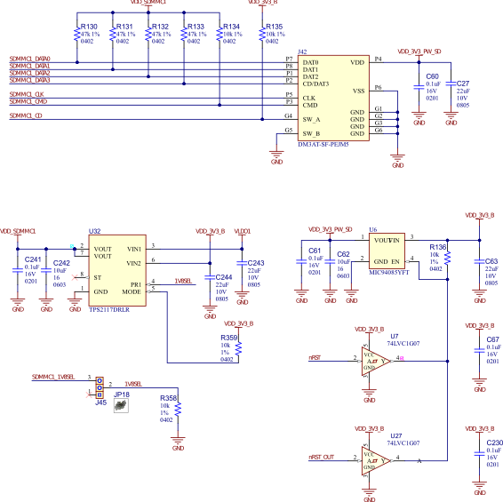
A 4-bit microSD card connector, J42, connected to the SDMMC1 interface, is mounted on the top side of the board. SDMMC1 communication is based on an 8-pin interface consisting of clock, command, four data and power lines. It also includes card detect and write-protect switches.
The SDMMC1 connector enables the system to boot from an SD card, provided that the correct binary file is copied to the root level of the card.
The SDMMC reset is triggered by the system reset signal, which cycles the SD card power through the MIC94085YFT high-side load switch. For more information about the MIC94085YFT device, refer to the product web page.
PIO | Signal Name | Signal Description |
|---|---|---|
PC04 | SDMMC1_CD | SD card detection |
PB30 | SDMMC1_CLK | SDIO clock |
PB29 | SDMMC1_CMD | SDIO command |
PB31 | SDMMC1_DATA0 | SDIO data bit 0 |
PC00 | SDMMC1_DATA1 | SDIO data bit 1 |
PC01 | SDMMC1_DATA2 | SDIO data bit 2 |
PC02 | SDMMC1_DATA3 | SDIO data bit 3 |
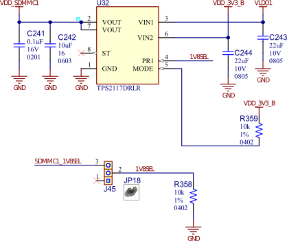
The SDMMC1 interface supports switching the I/O voltage level from 3.3V to 1.8V to enable High-Speed modes for the SD card.
When jumper JP18 is set across pins 2-3 of header J45, the SAMA7G54 MPU can dynamically control switching by asserting the PC05 PIO high to select 1.8V if a card supporting High-Speed modes is detected (depending on software support).
When jumper JP18 is set across pins 1-2 of header J45, 3.3V operation (legacy speed) is permanently selected.
The schematic below shows the circuit that selects the 3.3V or 1.8V supply voltage using the TPS2117DRLR power multiplexer.