
8.7.3 Multichip Simulation
System designs are typically divided into functional modules implemented by several Actel devices. To check the functionality of the system, you must simulate all Actel devices together. You can use ViewSim and Designer to perform multichip simulation. Use the following procedure to perform a multichip simulation of an Actel design:
- Create a top-level schematic and instantiate the individual chip
designs. This example assumes there are three designs with instance names “chip1,”
“chip2,” and “chip3.” The name of the top-level schematic is “top.” The following
figure depicts the directory structure for this example. Names written in normal
text represent file names and those in bold text represent directory names.
Figure 8-6. Directory Structure for Multichip Simulation 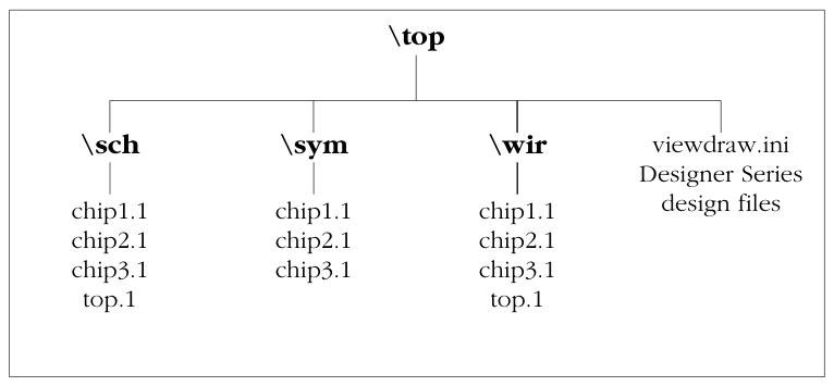 Note: This example only contains single-sheet schematics for each design. Similar procedures apply to multiple-sheet designs.
 - Place-and-route your design in Designer. For information about using Designer, see the Using Designer Guide.
- Extract timing information for your
design. From the File menu, select . Choose the format (SDF is most common), name your file
<design_name>.SDF, and click Save to continue. - Back annotate your delays. Click the back annotate button in the
Designer menu. The Open dialog box is displayed. Select
the
chip1.sdffile and click OK to generate thechip1.dtbfile. Repeat for thechip2.dtbandchip3.dtbfiles. - Generate a “top.dtb” file for the
top-level schematic. The top-level DTB file includes the following
lines:
.ba
c chip1
a dtb=chip1.dtb
c chip2
a dtb=chip2.dtb
c chip3
a dtb=chip3.dtb
.ab
The
cline above specifies an instance name,chip1. If you have not labeled an instance, use the default handle name of an instance,$1I38as it appears in your top-level schematic. Also, the individual DTB files reside in the top-level design directory,top. - Run ViewVSM on
top.dtb. Reference thetop.dtbfile in the VSM pop-up dialog box. The VSM program processes the DTB files for each chip and creates thetop.vsmfile with back-annotated postlayout timing delays. - Simulate
top.vsm. Invoke ViewSim. Typetop.vsmin the Design Name box and click OK.
For more information about performing simulation with ViewSim, see the Innoveda documentation.