Use the multi-layer host board for routing signals on the inner layer and the bottom layer.
The top layer (underneath the module) of the host board must be grounded with as many GND vias as possible.
Avoid fan-out of the signals under the module or antenna area. Use a via to fan-out signals to the edge of the PIC32WM-BZ6 Module.
For a better GND connection to the PIC32WM-BZ6 Module, solder the exposed GND pads of the PIC32WM-BZ6 Module on the host board.
For the module GND pad, use a GND via of a minimum 10 mil (hole diameter) for good ground to all the layers and thermal conduction path.
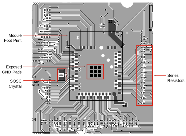
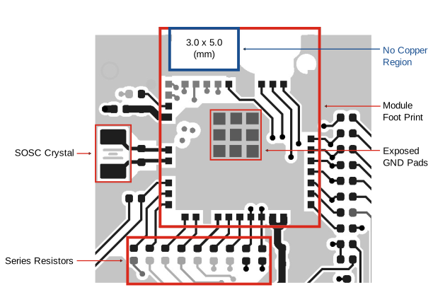
The recommendation is to add a series resistor on the host board for GPIOs, mainly
critical high-frequency pins and clocks for EMI considerations. The actual pin
configuration determines the value of the series resistor. The user must place these
resistors close to the PIC32WM-BZ6 Module. The
following figures illustrate the placement of the series resistor.
Place the SOSC crystal (32.768 kHz) on the host board close to the PIC32WM-BZ6 Module and follow the shortest trace routing length with no vias.
USB differential pair signals are 90Ω impedance
controlled on the PIC32WM-BZ6204 Module PCB and the same
must be followed on the host board.
Figure 5-9. Example of Host Board on Top
Layer – PIC32WM-BZ6204 Module
Figure 5-10. Example of Host Board on Top Layer – PIC32WM-BZ6602
Module
DS00005998E
The online versions of the documents are provided as a courtesy. Verify all content and data in the device’s PDF documentation found on the device product page.