
2.8.1 Configurator
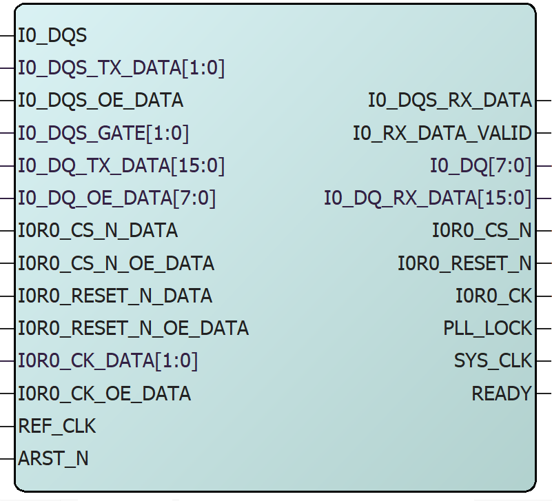
(Ask a Question)The following figure shows the main GUI window of the Octal DDR PHY Configurator.

The following table lists the Octal DDR PHY Configurator options and parameters.
| Parameter | Range | Description |
|---|---|---|
| PROTOCOL | XSPI | Protocol used to build the PHY |
| ONFI | ||
| HYPERBUS | ||
| APMEMORY_PSRAM | ||
| CLOCK_FREQ | 1-250 MHz | Memory clock frequency |
| CLOCK_TYPE | SINGLE_ENDED | 1 clock |
| DIFFERENTIAL | True differential clock pair | |
| PSEUDO_DIFFERENTIAL | Two single ended clocks in phase opposition | |
| Enable Differential DQS | — | This option is available for ONFI, HyperBus, and APMemory PSRAM protocols. When this option is selected, differential DQS bidirectional ports are exposed for DQS IOD. This option is required for interfacing to an external flash or NVDDR RAM at more than 200 MHz. |
| NUMBER_OF_DQ | 4 or 8 | Number of DQ bits |
| EXPOSE_DQ_RAW_DATA | 0–1 | When 1, this adds I*_DQ_RAW_DATA output to the fabric. Direct connection of DQ input to the fabric bypassing the PHY. It can be used to sample input data in 1-1-1 mode for xSPI. |
| FABRIC_CLOCK_RATIO | FULL | In full rate, the fabric run at the memory frequency. |
| CCC_PLL_MULTIPLIER | 1–39 | Multiplication factor from the external reference clock to the memory frequency. |
| CCC_PLL_REF_FREQ | — | Resulting reference clock frequency |
| DQS_DELAY_TAP | 1 - 255 | Delay tap set on DQS for read. Libero default value of 70 is optimized for 200 MHz performance if PCB routing is closely matched. Value below 20 fails in simulation. |
| INTERFACE_NB | 1–8 | Number of shared interface |
| RANK_NB | 1–4 | Number of rank per interface |
| I{INTERFACE#}R{RANK#}_{IO}_ENABLED | 0–1 | For all I/O except DQ/DQS: Expose the I/O and
corresponding signals. It can be used to disable I/O that are optional in the
protocol (RESET_N for instance) or that are shared between interfaces/ranks. This parameter is set using the related I/O Sharing tab in the Configurator. |
| I{INTERFACE#}R{RANK#}_{IO}_IN_DQ_LANE | 0–1 | For all I/O except DQ/DQS: Indicates that,
the corresponding I/O will be placed in the DQ Lane. P and R will fail if an
I/O is placed in DQ/DQS lane if this parameter is not set. By default, we
assume all I/O other than DQ/DQS outside of the DQ/DQS lane. This parameter is set using the related I/O Placement tab in the Configurator. |
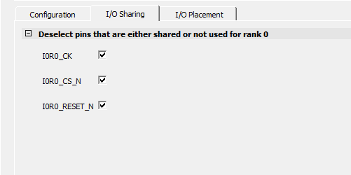
The I/O Sharing tab sets the (I{INTERFACE#}R{RANK#}_{IO}_ENABLED parameter for CK, CS_N, INT_N, and RESET_N/RSTO pins allowing the user to deselect a port of the interface. Once set, that port would not be in the generated netlist. This is used to deselect the not used in the design or a port that is tied-off (that is, INT# input of HypeRAM), or for multi-rank deselect ports that are shared between ranks.
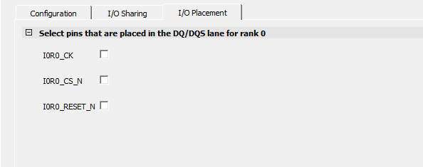
The I{INTERFACE#}R{RANK#}_{IO}_IN_DQ_LANE parameter is set with the I/O Placement tab in the configurator. It is used to indicate that a CK, CS_N, and RESET ports are in the DQ lane enabling Libero to correctly optimize the connections.
| Port | Width | Direction | Visibility | Description | Notes |
|---|---|---|---|---|---|
| General | |||||
| REF_CLK | 1 | IN | — | Reference clock to the CCC. It must be at CCC_PLL_REF_FREQ frequency. | — |
| ARST_N1 | 1 | IN | — | Asynchronous reset to the PHY. Note that, while ARST_N is asserted, the CCC inside the PHY is powerdown. | — |
| PLL_LOCK | 1 | OUT | — | Internal CCC PLL lock. | — |
| SYS_CLK | 1 | OUT | — | System clock. All input/output of the PHY from/to the fabric are synchronous to this clock (unless mentioned otherwise). SYS_CLK is generated by OUT0 of the CCC through CLKINT. | — |
| READY | 1 | OUT | — | When high indicates that the PHY initialization is complete and can receive commands. | — |
| Output | Clock can be any of: C, SCK, CK, CLK depending on protocol. | — | |||
| I{INTERFACE#}R{RANK#}_{CLOCK} | 1 | OUT | I{INTERFACE#}R{RANK#}_{CLOCK}_ENABLED== 1. This parameter is set using the related I/O Sharing tab in the Configurator. | Output pad to the memory, DDR. | CCC OUT1 through HS_IO_CLK, 90deg phase shift |
| I{INTERFACE#}R{RANK#}_{CLOCK}_N | 1 | OUT | I{INTERFACE#}R{RANK#}_{CLOCK}_ENABLED== 1. Protocol dependent. This parameter is set using the related I/O Sharing tab in the Configurator. | Output pad N side to the memory, DDR. | CCC OUT1 through HS_IO_CLK, 90deg phase shift |
| I{INTERFACE#}R{RANK#}_{CLOCK}_DATA | 2 | IN | I{INTERFACE#}R{RANK#}_{CLOCK}_ENABLED== 1. This parameter is set using the related I/O Sharing tab in the Configurator. | 2-bit port.
| SYS_CLK |
| I{INTERFACE#}R{RANK#}_{CLOCK}_OE_DATA | 2 | IN | I{INTERFACE#}R{RANK#}_{CLOCK}_ENABLED == 1. This parameter is set using the related I/O Sharing tab in the Configurator. | Output enable data from the fabric to the I/O pad. See the timing section for the latency through the PHY. | SYS_CLK |
| Command | Output can be any of: S_N, CS_N, CE_N, RESET_N, ALE, CLE, WR_N, WP_N. | ||||
| I{INTERFACE#}R{RANK#}_{OUTPUT} | 1 | OUT | I{INTERFACE#}R{RANK#}_{OUTPUT}_ENABLED == 1. This parameter is set using the related I/O Sharing tab in the Configurator. | Output pad to the memory, SDR. | CCC OUT0 through HS_IO_CLK |
| I{INTERFACE#}R{RANK#}_{OUTPUT}_DATA | 1 | IN | I{INTERFACE#}R{RANK#}_{OUTPUT}_ENABLED== 1. This parameter is set using the related I/O Sharing tab in the Configurator. | Output data from the fabric to the I/O pad. See the timing section for the latency through the PHY. | SYS_CLK |
| I{INTERFACE#}R{RANK#}_{OUTPUT}_OE_DATA | 1 | IN | I{INTERFACE#}R{RANK#}_{OUTPUT}_ENABLED== 1. This parameter is set using the related I/O Sharing tab in the Configurator. | Output enable data from the fabric to the I/O pad. See the timing section for the latency through the PHY. | SYS_CLK |
| Asynchronous Inputs | |||||
| I{INTERFACE#}R{RANK#}_{INPUT} | 1 | IN | I{INTERFACE#}R{RANK#}_{INPUT}_ENABLED == 1. This parameter is set using the related I/O Sharing tab in the Configurator. | Input pad from the memory. | ASYNC |
| I{INTERFACE#}R{RANK#}_{INPUT}_DATA | 1 | OUT | I{INTERFACE#}R{RANK#}_{INPUT}_ENABLED == 1. This parameter is set using the related I/O Sharing tab in the Configurator. | Input data to the fabric. | ASYNC |
| DQS | |||||
| I{INTERFACE#}_{DQS} | 1 | INOUT | — | Inout pad from/to the memory, DDR. | CCC OUT0 through HS_IO_CLK |
| I{INTERFACE#}_{DQS}_N | 1 | INOUT | Protocol dependent | Inout pad N side from/to the memory, DDR. | CCC OUT0 through HS_IO_CLK |
| I{INTERFACE#}_{DQS}_TX_DATA | 2 | IN | protocol !=XSPI | Output data from the fabric to the I/O pad. See the timing section for the latency through the PHY. | SYS_CLK |
| I{INTERFACE#}_{DQS}_OE_DATA | 2 | IN | — | Output enable data from the fabric to the I/O pad. See the timing section for the latency through the PHY. | SYS_CLK |
| I{INTERFACE#}_{DQS}_RX_DATA | 1 | OUT | — | Input data from the I/O pad to the fabric. Asynchronous. It is not gated by the GATE signal. Note that, this signal will toggle when DQS is driven by the fabric. | ASYNC |
| I{INTERFACE#}_{DQS}_GATE | 2 | IN | — | DQS gating signal to the PHY. It is used to gate DQS going into the PHY RX FIFO. The gate must be low when the memory does not drive strobes (must be low whenever DQS is 'bZ or one DQS is driven by the FPGA or when DQS from the memory is not strobe. See timing section for the latency. | SYS_CLK |
| DQ | |||||
| I{INTERFACE#}_DQ | 4 or 8 | INOUT | — | Inout pad to the memory, DDR INOUT except for XSPI where it is IN DQS can be any of: DQS, DS, and RWDS depending on protocol. | CCC OUT0 through HS_IO_CLK |
| I{INTERFACE#}_DQ_TX_DATA | 8 or 16 | IN | protocol !=XSPI | Output data from the fabric to the I/O pad. See the timing section for the latency through the PHY. | SYS_CLK |
| I{INTERFACE#}_DQ_OE_DATA | 4 or 8 | IN | — | Output enable data from the fabric to the I/O pad. See the timing section for the latency through the PHY. | SYS_CLK |
| I{INTERFACE#}_DQ_RX_DATA | 8 or 16 | OUT | — | Input data from the I/O pad to the fabric. Synchronous. See the timing section for the latency through the PHY. | SYS_CLK |
| I{INTERFACE#}_RX_DATA_VALID | 1 | OUT | — | Indicate that received data are valid. | SYS_CLK |
| I{INTERFACE#}_DQ_RX_RAW_DATA | 4 or 8 | OUT | — | Input data from the I/O pad to the fabric. Asynchronous. This port will also toggle when DQ is driven by the fabric. | ASYNC |
- The ARST_N signal is not internally synchronized to the REF_CLK signal in the PF_IOD_OCTAL_DDR IP. Thus, as good design practice, synchronize the ARST_N signal in the fabric, and then, define a false path constraint for any paths traversing through the reset synchronizer.

