
46.10.5 Analog-to-Digital Converter (ADC) Characteristics
| Symbol | Parameters | Conditions | Min. | Typ. | Max. | Unit |
|---|---|---|---|---|---|---|
| RES | Resolution | - | - | - | 12 | bits |
| Conversion speed | - | 10 | - | 1000 | ksps | |
| fs | Sampling clock | - | 10 | - | 1000 | kHz |
| clk | ADC Clock frequency | - | - | fs.16 | - | Hz |
| TS | Sampling time | OFFCOMP=1 | 250 | - | 25000 | ns |
| Conversion range | Diff mode | -VREF | - | VREF | V | |
| Single-Ended mode | 0 | - | VREF | |||
| VREF | Reference input | REFCOMP=1 | 1 | - | VDDANA-0.6 | V |
| REFCOMP=0 | VDDANA | - | VDDANA | |||
| VIN | Input channel range | - | 0 | - | VDDANA | V |
| VCMIN | Input common mode voltage | For VREF > 1.0V | 0.7 | - | VREF-0.7 | V |
| For VREF=1.0V | 0.3 | - | VREF-0.3 | |||
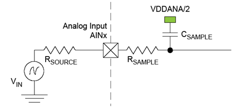
| CSAMPLE(1) | Input sampling capacitance | - | - | 2.8 | 3.2 | pF |
| RSAMPLE(1) | Input sampling on-resistance | - | - | - | 1715 | Ω |
| Rref(1) | Reference input source resistance | REFCOMP=1 | - | - | 5 | kΩ |
- These values are based on simulation. They are not covered by production test limits or characterization.
- The ADC channels on pins PB00, PB01, PB02 and PB03 are powered, depending on VSWOUT, from the VDDIN or VBAT power supply. The ADC performance of these pins will be lower than on all the other ADC channels on pins powered from the VDDANA power supply.
| Symbol | Parameters | Conditions | Ta | Min. | Typ. | Max. | Unit |
|---|---|---|---|---|---|---|---|
| IDDANA | Differential Mode |
fs=1Msps / Reference buffer disabled |
Max.85°C | - | 105 | 128 | µA |
|
fs=1Msps / Reference buffer disabled | - | 279 | 307 | ||||
| Differential Mode |
fs=1Msps / Reference buffer enabled | - | 175 | 231 | µA | ||
|
fs=1Msps / Reference buffer enabled | - | 300 | 374 | ||||
|
fs=1Msps / Reference buffer enabled | - | 356 | 438 | ||||
| Differential Mode |
fs=10ksps / Reference buffer disabled | - | 30 | 41 | µA | ||
|
fs=10ksps / Reference buffer disabled | - | 53 | 71 | ||||
| Differential Mode |
fs=10ksps / Reference buffer enabled | - | 95 | 139 | µA | ||
|
fs=10ksps / Reference buffer enabled | - | 115 | 178 | ||||
|
fs=10ksps / Reference buffer enabled | - | 122 | 187 | ||||
| IDDANA | Single-Ended Mode |
fs=1Msps / Reference buffer disabled |
Max.85°C | - | 138 | 158 | µA |
|
fs=1Msps / Reference buffer disabled | - | 321 | 359 | ||||
| Single-Ended Mode |
fs=1Msps / Reference buffer enabled | - | 203 | 257 | µA | ||
|
fs=1Msps / Reference buffer enabled | - | 331 | 413 | ||||
|
fs=1Msps / Reference buffer enabled | - | 388 | 482 | ||||
| Single-Ended Mode |
fs=10ksps / Reference buffer disabled | - | 46 | 62 | µA | ||
|
fs=10ksps / Reference buffer disabled | - | 89 | 120 | ||||
| Single-Ended Mode |
fs=10ksps / Reference buffer enabled | - | 109 | 157 | µA | ||
|
fs=10ksps / Reference buffer enabled | - | 138 | 211 | ||||
|
fs=10ksps / Reference buffer enabled | - | 148 | 228 |
| Symbol | Parameters | Conditions | Min. | Typ. | Max. | Unit |
|---|---|---|---|---|---|---|
| ENOB | Effective Number of bits | VDDANA=3.0V / Vref =2.0V | 9.6 | 10.5 | 10.6 | bits |
| VDDANA=1.6V/3.6V Vref=1.0V | 8.9 | 9.7 | 9.9 | |||
| VDDANA=Vref=1.6V | 10 | 10.5 | 11.1 | |||
| VDDANA=Vref=3.6V | 10.5 | 10.9 | 11.0 | |||
| TUE | Total Unadjusted Error | VDDANA=3.0V, Vref=2.0V | - | 7.5 | 11 | LSB |
| INL | Integral Non Linearity | VDDANA=3.0V, Vref=2.0V | - | +/-1.5 | +/-2.1 | LSB |
| DNL | Differential Non Linearity | VDDANA=3.0V, Vref=2.0V | - | +/-0.8 | +1.1/-1.0 | LSB |
| Gain Error | External Reference voltage 1.0V | - | +/-0.7 | +/-1.5 | % | |
| External Reference voltage 3.0V | - | +/-0.2 | +/-0.5 | |||
| Reference bandgap voltage | - | +/-0.4 | +/-4.4 | |||
| VDDANA | - | +/-0.1 | +/-0.4 | |||
| VDDANA/2 | - | +/-0.4 | +/-1.3 | |||
| VDDANA/1.6 | - | +/-0.3 | +/-0.9 | |||
| Offset Error | External Reference voltage 1.0V | - | +/-1.1 | +/-2.4 | mV | |
| External Reference voltage 3.0V | - | +/-1.1 | +/-3 | |||
| Reference bandgap voltage | - | +/-2.3 | +/-7.5 | |||
| VDDANA | - | +/-0.9 | +/-2.9 | |||
| VDDANA/2 | - | +/-1 | +/-2.6 | |||
| VDDANA/1.6 | - | +/-1 | +/-2.9 | |||
| SFDR | Spurious Free Dynamic Range | Fs=1MHz / Fin=13 kHz / Full range Input signal VDDANA=3.0V, Vref=2.0V | 68 | 75 | 77 | dB |
| SINAD | Signal to Noise and Distortion ratio | 60 | 65 | 66 | ||
| SNR | Signal to Noise ratio | 61 | 66 | 67 | ||
| THD | Total Harmonic Distortion | -74 | -73 | -67 | ||
| Noise RMS | External Reference voltage | - | 1.0 | 2.5 | mV |
| Symbol | Parameters | Conditions | Min. | Typ. | Max. | Unit |
|---|---|---|---|---|---|---|
| ENOB | Effective Number of bits | VDDANA=3.0V / Vref =2.0V | 8.5 | 9.5 | 9.8 | bits |
| VDDANA=1.6V/3.6V Vref=1.0V | 7.5 | 8.7 | 8.9 | |||
| VDDANA=Vref=1.6V (2) | 9.0 | 9.5 | 9.8 | |||
| VDDANA=Vref=3.6V | 9.2 | 9.8 | 9.9 | |||
| TUE | Total Unadjusted Error | VDDANA=3.0V, Vref=2.0V | - | 17.4 | 31 | LSB |
| INL | Integral Non Linearity | VDDANA=3.0V, Vref=2.0V | - | +/-2.2 | +/-10.1 | LSB |
| DNL | Differential Non Linearity | VDDANA=3.0V, Vref=2.0V | - | +/-0.8 | +/-0.9 | LSB |
| Gain Error | External Reference voltage 1.0V | - | +/-1 | +/-1.3 | % | |
| External Reference voltage 3.0V | - | +/-0.3 | +/-0.6 | |||
| Reference bandgap voltage | - | +/-0.4 | +/-3.2 | |||
| Vref=VDDANA (2) | - | +/-0.1 | +/-0.3 | |||
| Vref=VDDANA/2 | - | +/-0.6 | +/-1.4 | |||
| Vref=VDDANA/1.6 | - | +/-0.4 | +/-1 | |||
| Offset Error | External Reference voltage 1.0V | - | +/-3.4 | +/-13 | mV | |
| External Reference voltage 3.0V | - | +/-3.6 | +/-24 | |||
| Reference bandgap voltage | - | +/-1 | +/-14 | |||
| Vref=VDDANA (2) | - | +/-4.2 | +/-25 | |||
| Vref=VDDANA/2 | - | +/-5.7 | +/-10 | |||
| Vref=VDDANA/1.6 | - | +/-6.3 | +/-13 | |||
| SFDR | Spurious Free Dynamic Range | Fs=1MHz / Fin=13kHz / Full range Input signal VDDANA=3.0V, Vref=2.0V | 65 | 71 | 78 | dB |
| SINAD | Signal to Noise and Distortion ratio | 53 | 59 | 61 | ||
| SNR | Signal to Noise ratio | 53 | 59 | 61 | ||
| THD | Total Harmonic Distortion | -76 | -70 | -64 | ||
| Noise RMS | External Reference voltage | - | 2.0 | 7.0 | mV |
- These values are based on characterization.
- All parameters given above exclude the corner VDDANA = Vref = 1.6V, Ta = -40°C.
For 12-bit accuracy: