
2.3.7 How To Set Up Design and Memory Initialization
(Ask a Question)This section describes how to initialize PCIe, transceivers, and fabric RAM blocks using the Configure Design Initialization Data and Memories option in Libero SoC. Design and Memory Initialization is divided into three stages of initialization as shown in the following figure.

- The first stage client is responsible for the bring-up of FPGA fabric and related IOs, and then de-asserts the FABRIC_POR_N signal. This client is stored in the sNVM at the top of the address space.
- The second stage client initializes the PCIe and XCVR blocks present in the design. The client is stored in the sNVM and the starting address of the client is configurable.
- The third stage client initializes the fabric RAMs present in the design. Each logical RAM in the design can be initialized from a different Storage Type—sNVM, µPROM, or SPI Flash. The starting address of these storage types is configurable.
- Broadcast instructions to initialize RAMs to zeros option initializes all RAM blocks to zeros before the FABRIC_POR_N signal is asserted. On enabling this option, the physical instances with zero data in stage 2_3 or stage_3 assembly files are filtered out.
- The second stage client initializes the PCIe and XCVR blocks present in the design. Import a text file to change the default PCIe/XCVR register values (custom configuration). This modifies the Stage 2 generated assembly file (from default flow). The format in the text file to change the register content is as follows: Instance_Name, Register:Field_Name, and Hex value separated by spaces. For example: PF_PCIE_0/PCIESS_LANE0_Pipe_AXI0 SER_DRV_CTRL:TXDRVTRIM 0xFFFFFF
- When initializing RAM from SPI Flash, ensure that the System Controller SPI interface is in the Master mode by setting the IO_CFG_INTF pin to 1.
- The SPI Clock divider value specifies the required SPI SCK frequency to read the initialization data from SPI Flash. The SPI Clock divider value must be selected based on the external SPI Flash operating frequency range.
- SPI part for the PolarFire and RT PolarFire FPGA is MT25QU01GBBB and for the PolarFire SoC and RT PolarFire SoC FPGA is MT25QL01GBBB. Flash is connected to Bank 6 (1.8V) on the PolarFire and RT PolarFire FPGA and Bank 3 (3.3V) on the PolarFire SoC and RT PolarFire SoC FPGA.
| SPI Clock Divider Value | SCK Frequency |
|---|---|
| 2 | 40 MHz |
| 4 | 20 MHz |
| 6 | 13.3 MHz |
Follow these steps to initialize fabric RAMs at power-up:
- Select the required logical RAM from the Fabric RAMs tab and click Edit. The Edit Fabric RAM Initialization Client window provides the following options to:
- Initialize the client from an Intel-Hex (*.hex), Simple-Hex(*.shx), Motorola-S (*.s), or Microchip Binary (*.mem)
- Initialize the client with Zeros
- Create the client as a placeholder with no content
- Select Storage Type for the client
Figure 2-10. Fabric RAMs 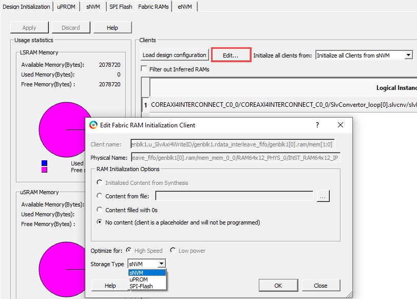
- After configuring the RAM initialization client, click Apply on the Fabric RAMs tab.
- Select Generate Design Initialization Data
under the Design Flow tab. It automatically generates the first, second, and
third stage initialization clients, which are automatically added to the
non-volatile memory that the user chooses.
The Generate Design Initialization Data is highlighted as shown in the following figure.
Figure 2-11. Generate Design Initialization Data 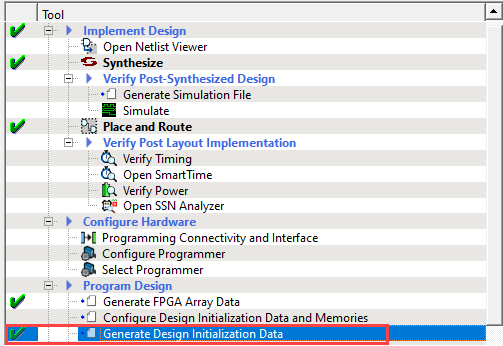
The initialization clients are added to the respective tab; µPROM, SNVM, SPI Flash, or eNVM (for PolarFire SoC and RT PolarFire SoC FPGA only). When plaintext or ciphertext authenticated clients are added, Initialize sNVM Master Key option is enabled and grayed out, as shown in the following figure.
Figure 2-12. Initialization Clients Generated in sNVM  Important: The second stage client is added to sNVM if the user design includes the PCIe or XCVR block.
The following figure shows the Configure Bitstream dialog, which is updated as per the sNVM configurations.
Figure 2-13. Configure Bitstream 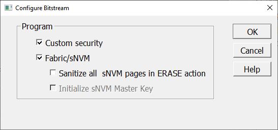
If SPI Flash is selected as the storage type, the initialization client is added to the SPI Flash tab as shown in the following figure.
Figure 2-14. Third Initialization Client on SPI Flash 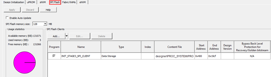
- If an external SPI Flash is chosen for stage 3, before completing the Run PROGRAM Action, you should generate Generate SPI Flash Image and Run PROGRAM_SPI_IMAGE Action from the Design Flow tab, as shown in the following figure.
Figure 2-15. Program SPI Flash Image 
These steps ensure that PCIe, XCVR, and Fabric RAMs present in the design are initialized during power-up using initialization clients placed in the non-volatile memory based on the user selection.