
6.5 Configure Design Initialization Data and Memories
(Ask a Question)The Configure Design Initialization Data and Memories option creates the LSRAM initialization client. When the PolarFire device powers up, the LSRAM memory is initialized with the sNVM contents.
To create the LSRAM initialization client, perform the following steps:
On the Design Flow tab, double click Configure Design Initialization Data and Memories, as shown in the following figure.
Figure 6-2. Configure Design Initialization Data and Memories Option 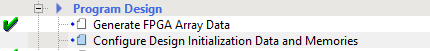
- In the Configure Design Initialization
Data and Memories window, select the Fabric RAMs tab,
and then select the pf_sram file to import the memory information, as
shown in the following figure.
Figure 6-3. Fabric RAMs Tab 
- Import the hex file
(
gbe_webserver.hexfor webserver design andgbe_tftp_iap.hexfor TFTP_IAP design) provided with the design files from
ormpf_an4569_v2023p2_eval_df\webserver\TCL_Scripts\src\src_softconsole\gbe_webserver.hexmpf_an4569_v2023p2_eval_df\tftp_iap\TCL_Scripts\src\src_softconsole\gbe_tftp_iap.hexThe
gbe_webserver.hexorgbe_tftp_iap.hexfile is a application file generated using SoftConsole that configures the ZL clock generation hardware, the CoreTSE_AHB registers, and the VSC PHY. The application code is initially stored in an external SPI Flash. On device power-up, the system controller copies the code to LSRAM from external SPI Flash, and the Mi-V processor executes the code from LSRAM. To ensure that the fabric LSRAM contents are stored in the external SPI Flash, select Storage Type as SPI Flash, see in Figure 6-3. - Click Apply.
- Select Start address for SPI Flash
clients and SPI Clock divider value, in the
Design Initialization tab as shown in the following figure.
Figure 6-4. Start Address for SPI Flash Clients  Note: The default start address for SPI-Flash clients 0x400 is used for the webserver design. The start address for TFTP design is modified to 0x2000. This is required to support Flash erase of 4 KB while writing the SPI directory into initial SPI Flash 1 KB memory using design firmware.
 - On the Design Flow tab,
double click Generate Design Initialization Data.
When the LSRAM initialization client is successfully generated in sNVM, a green tick appears next to Generate Design Initialization Data, as shown in Figure 6-1.
When the device is programmed, the LSRAM block is initialized from the sNVM.