
46.11.4 Analog-to-Digital Converter (ADC) Characteristics
| Symbol | Parameters | Conditions | Min. | Typ. | Max. | Unit |
|---|---|---|---|---|---|---|
| Res | Resolution | - | - | 12 | bits | |
| Rs | Sampling rate(2) | resolution 12 bit (RESSEL = 0) and SAMPLEN = 3 | 10 | - | 1000 | ksps |
| Nb_cycles | Differential mode Number of ADC clock cycles SAMPCTRL.OFFCOMP = 1 | resolution 12 bit (RESSEL = 0) | - | 16 | - | cycles |
| resolution 10 bit (RESSEL = 2) | 14 | |||||
| resolution 8 bit (RESSEL = 3) | 12 | |||||
| Differential mode Number of ADC clock cycles SAMPCTRL.OFFCOMP = 0 SAMPLEN corresponds to the decimal value of SAMPLEN[5:0] | resolution 12 bit (RESSEL = 0) | - | SAMPLEN+13 | - | cycles | |
| resolution 10 bit (RESSEL = 2) | SAMPLEN+11 | |||||
| resolution 8 bit (RESSEL = 3) | SAMPLEN+9 | |||||
| Single-ended mode Number of ADC clock cycles SAMPCTRL.OFFCOMP = 1 | resolution 12 bit (RESSEL = 0) | - | 16 | - | cycles | |
| resolution 10 bit (RESSEL = 2) | 15 | |||||
| resolution 8 bit (RESSEL = 3) | 13 | |||||
| Single-ended mode Number of ADC clock cycles SAMPCTRL.OFFCOMP = 0 SAMPLEN corresponds to the decimal value of SAMPLEN[5:0] | resolution 12 bit (RESSEL = 0) | - | SAMPLEN+13 | - | cycles | |
| resolution 10 bit (RESSEL = 2) | SAMPLEN+12 | |||||
| resolution 8 bit (RESSEL = 3) | SAMPLEN+10 | |||||
| fadc | ADC Clock frequency | - | 160 | - | 16000 | kHz |
| Ts | Sampling time | SAMPCTRL.OFFCOMP = 1 | 250 | - | 25000 | ns |
| SAMPCTRL.OFFCOMP = 0 | (SAMPLEN+1) / fadc | - | - | s | ||
| Sampling time with DAC as input (MUXPOS = 0x1C) | 3000 | - | - | ns | ||
| Sampling time with Bandgap as input (MUXPOS = 0x19) | 10000 | - | - | |||
| - | Conversion range | Diff mode | -Vref | - | Vref | V |
| - | Conversion range | Single-ended mode | 0 | - | Vref | |
| Vref | Reference input | 1 | VDDANA-0.6 | V | ||
| Vin | Input channel range | - | 0 | - | VDDANA | V |
| Vcmin | Input common mode voltage | For Vref > 1.0V | 0.7 | - | Vref-0.7 | V |
| For Vref = 1.0V | 0.3 | - | Vref-0.3 | V | ||
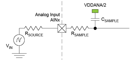
| CSAMPLE(1) | Input sampling capacitance | - | 2.8 | 3.2 | pF | |
| RSAMPLE(1) | Input sampling on-resistance | - | - | 1715 | Ω | |
| Rref(1) | Reference input source resistance | REFCOMP = 1 | - | - | 5 | kΩ |
Note:
- These values are based on simulation. They are not covered by production test limits or characterization.
- Sampling rate (in samples per second) is equal to Nb_cycles/fadc.
| Symbol | Parameters | Conditions | Measurements | Unit | |||
|---|---|---|---|---|---|---|---|
| Min | Typ | Max | |||||
| ENOB | Effective Number of bits | Fadc = 1Msps | Vref = 2.0V Vddana = 3.0V | 9.1 | 10.2 | 10.8 | bits |
| Vref = 1.0V Vddana = 1.62V to 3.6V | 9.0 | 10.1 | 10.6 | ||||
| Vref = Vddana = 1.62V to 3.6V | 8.9 | 9.9 | 11.0 | ||||
| Bandgap Reference, Vddana = 1.62V to 3.6V | 9.0 | 9.8 | 10.6 | ||||
| TUE | Total Unadjusted Error | without offset and gain compensation | Vref = Vddana = 1.62V to 3.6V | - | 7 | 32 | LSB |
| INL | Integral Non Linearity | without offset and gain compensation | Vref = Vddana = 1.62V to 3.6V | - | +/-1.9 | +/-4 | |
| DNL | Differential Non Linearity | without offset and gain compensation | Vref = Vddana = 1.62V to 3.6V | - | +0.94/-1 | +1.85/-1 | |
| Gain | Gain Error | without gain compensation | Vref = 1V Vddana = 1.62V to 3.6V | - | +/-0.38 | +/-1.9 | % |
| Vref = 3V Vddana = 1.62V to 3.6V | - | +/-0.14 | +/-0.9 | ||||
| Bandgap Reference | - | +/-0.64 | +/-5.4 | ||||
| Vref = Vddana = 1.62V to 3.6V | - | +/-0.15 | +/-0.9 | ||||
| Offset | Offset Error | without offset compensation | Vref = 1V Vddana = 1.62V to 3.6V | - | +/-0.13 | +/-15.8 | mV |
| Vref = 3V Vddana = 1.62V to 3.6V | - | +/-1.82 | +/-14.9 | ||||
| Bandgap Reference | - | +/-2.07 | +/-15.8 | ||||
| Vref = Vddana = 1.62V to 3.6V | - | +/-1.82 | +/-15.3 | ||||
| SFDR | Spurious Free Dynamic Range | Fs = 1MHz/Fin = 13 kHz/Full range Input signal | Vref = 2.0V Vddana = 3.0V | 58.1 | 70.5 | 77.5 | dB |
| SINAD | Signal to Noise and Distortion ratio | 56.7 | 63.4 | 66.5 | |||
| SNR | Signal to Noise ratio | 56.5 | 64.4 | 67.1 | |||
| THD | Total Harmonic Distortion | -74.7 | -68.7 | -57.7 | |||
| - | Noise RMS | External Reference voltage | - | 0.42 | - | mV | |
Note:
- These values are given without any ADC oversampling and decimation features enabled.
- These values are based on characterization. They are not covered in test limits in production.
| Symbol | Parameters | Conditions | Measurements | Unit | |||
|---|---|---|---|---|---|---|---|
| Min | Typ | Max | |||||
| ENOB | Effective Number of bits | Fadc = 1Msps | Vref = 2.0V Vddana = 3.0V | 8.0 | 9.3 | 9.7 | bits |
| Vref = 1.0V Vddana = 1.62V to 3.6V | 7.9 | 8.2 | 9.4 | ||||
| Vref = Vddana = 1.62V to 3.6V | 8.6 | 9.2 | 9.9 | ||||
| Bandgap Reference, Vddana = 1.62V to 3.6V | 7.8 | 8.4 | 8.9 | ||||
| TUE | Total Unadjusted Error | without offset and gain compensation | Vref = 2.0V Vddana = 3.0V | - | 12 | 63 | LSB |
| INL | Integral Non Linearity | without offset and gain compensation | Vref = 2.0V Vddana = 3.0V | - | +/-3.4 | +/-8.9 | |
| DNL | Differential Non Linearity | without offset and gain compensation | Vref = 2.0V Vddana = 3.0V | - | +0.9/-1 | +1.8/-1 | |
| Gain | Gain Error | without gain compensation | Vref = 1V Vddana = 1.62V to 3.6V | - | +/-0.3 | +/-5.1 | % |
| Vref = 3V Vddana = 1.62V to 3.6V | - | +/-0.3 | +/-5.1 | ||||
| Bandgap Reference | - | +/-0.4 | +/-5.1 | ||||
| Vref = Vddana = 1.62V to 3.6V | - | +/-0.2 | +/-0.8 | ||||
| Offset | Offset Error | without offset compensation | Vref = 1V Vddana = 1.62V to 3.6V | - | +/-2.6 | +/-45 | mV |
| Vref = 3V Vddana = 1.62V to 3.6V | - | +/-2.6 | +/-45 | ||||
| Bandgap Reference | - | +/-1.3 | +/-34 | ||||
| Vref = Vddana = 1.62V to 3.6V | - | +/-1.8 | +/-37 | ||||
| SFDR | Spurious Free Dynamic Range | Fs = 1MHz/ Fin = 13 kHz/Full range Input signal | Vref = 2.0V Vddana = 3.0V | 56.1 | 63.8 | 72.6 | dB |
| SINAD | Signal to Noise and Distortion ratio | 50.0 | 57.7 | 60.1 | |||
| SNR | Signal to Noise ratio | 51.9 | 58.3 | 59.8 | |||
| THD | Total Harmonic Distortion | -72.5 | -62.4 | -52.3 | |||
| Noise RMS | External Reference voltage | - | 0.80 | - | mV | ||
Note:
- These values are given without any ADC oversampling and decimation features enabled.
- These values are based on characterization. They are not covered in test limits in production.
For 12-bit accuracy: