These macros are useful in some radiation hostile applications. They sacri-fice area in
exchange for a lower single-event upset (SEU) rate caused by ion particle collisions. These
special cells use two combinational modules to implement a register instead of using the
dedicated registers in the array
(for RadHard Field
Programmable Gate Arrays, see the application note titled, Design
Techniques).
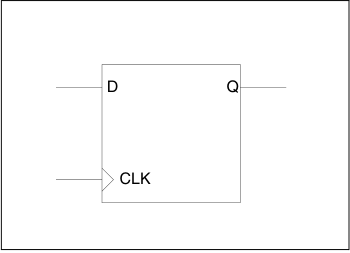
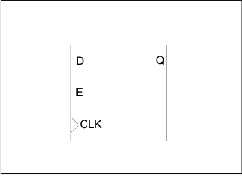
DF1_CC
This component is supported by ACT 2, ACT 3, 3200DX, MX, SX, SX-A, SX-S, eX families.
Figure 14-402. DF1_CC Logic Diagram
Function: D-Type Flip-Flop
Input: D, CLK
Output: Q
Table 14-706. Truth Table
CLK
Qn+1
↑
D
Table 14-707. Modules
Family
Seq
Comb
All
—
2
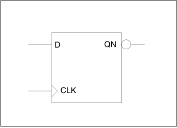
DF1A_CC
This component is supported by ACT 2, ACT 3, 3200DX, MX families.
Figure 14-403. DF1A_CC Logic Diagram
Function: D-Type Flip-Flop with active low Output
Input: D, CLK
Output: QN
Table 14-708. Truth Table
CLK
QNn+1
↑
!D
Table 14-709. Modules
Family
Seq
Comb
All listed
—
2
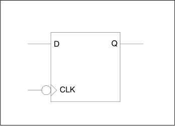
DF1B_CC
This component is supported by ACT 2, ACT 3, 3200DX, MX, SX, SX-A, SX-S, eX families.
Figure 14-404. DF1B_CC Logic Diagram
Function: D-Type Flip-Flop with active low Clock
Input: D, CLK
Output: Q
Table 14-710. Truth Table
CLK
Qn+1
↓
D
Table 14-711. Modules
Family
Seq
Comb
ACT 2, ACT 3, 3200DX, MX
—
2
SX, SX-A, SX-S, eX
1
—
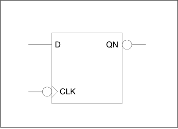
DF1C_CC
This component is supported by ACT 2, ACT 3, 3200DX, MX families.
Figure 14-405. DF1C_CC Logic Diagram
Function: D-Type Flip-Flop with active low Clock and Output
Input: D, CLK
Output: QN
Table 14-712. Truth Table
CLK
QNn+1
↓
!D
Table 14-713. Modules
Family
Seq
Comb
ACT 2, ACT 3, 3200DX, MX
—
2
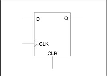
DFC1_CC
This component is supported by ACT 2, ACT 3, 3200DX, MX families.
Figure 14-406. DFC1_CC Logic Diagram
Function: D-Type Flip-Flop with active high Clear
Input: D, CLK, CLR
Output: Q
Table 14-714. Truth Table
CLR
CLK
Qn+1
1
X
0
0
↑
D
Table 14-715. Modules
Family
Seq
Comb
ACT 2, ACT 3, 3200DX, MX
—
2
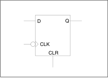
DFC1A_CC
This component is supported by ACT 2, ACT 3, 3200DX, MX families.
Figure 14-407. DFC1A_CC Logic Diagram
Function: D-Type Flip-Flop with active high Clear and active low Clock
Input: D, CLK, CLR
Output: Q
Table 14-716. Truth Table
CLR
CLK
Qn+1
1
X
0
0
↓
D
Table 14-717. Modules
Family
Seq
Comb
ACT 2, ACT 3, 3200DX, MX
—
2
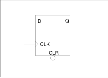
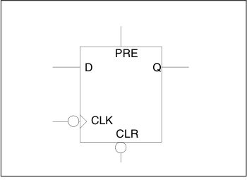
DFC1B_CC
This component is supported by ACT 2, ACT 3, 3200DX, MX, SX, SX-A, SX-S, eX families.
Figure 14-408. DFC1B_CC Logic Diagram
Function: D-Type Flip-Flop with active low Clear
Input: D, CLK, CLR
Output: Q
Table 14-718. Truth Table
CLR
CLK
Qn+1
0
X
0
1
↑
D
Table 14-719. Modules
Family
Seq
Comb
All listed
—
2
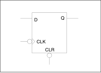
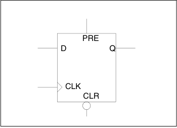
DFC1D_CC
This component is supported by ACT 2, ACT 3, 3200DX, MX, SX, SX-A, SX-S, eX families.
Figure 14-409. DFC1D_CC Logic Diagram
Function: D-Type Flip-Flop with active low Clear and Clock
Input: D, CLK, CLR
Output: Q
Table 14-720. Truth Table
CLR
CLK
Qn+1
0
X
0
1
↓
D
Table 14-721. Modules
Family
Seq
Comb
ACT 2, ACT 3, 3200DX, MX
—
2
SX, SX-A, SX-S, eX
1
—
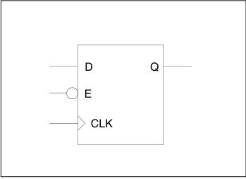
DFE_CC
This component is supported by ACT 2, ACT 3, 3200DX, MX families.
Figure 14-410. DFE_CC Logic Diagram
Function: D-Type Flip-Flop with active high Enable
Input: D, E, CLK
Output: Q
Table 14-722. Truth Table
E
CLK
Qn+1
0
X
Q
1
↑
D
Table 14-723. Modules
Family
Seq
Comb
ACT 2, ACT 3, 3200DX, MX
—
2
DFE1B_CC
This component is supported by ACT 2, ACT 3, 3200DX, MX, SX, SX-A, SX-S, eX families.
Figure 14-411. DFE1B_CC Logic Diagram
Function: D-Type Flip-Flop with active low Enable
Input: D, E, CLK
Output: Q
Table 14-724. Truth Table
E
CLK
Qn+1
1
X
Q
0
↑
D
Table 14-725. Modules
Family
Seq
Comb
ACT 2, ACT 3, 3200DX, MX
—
2
SX, SX-A, SX-S, eX
1
—
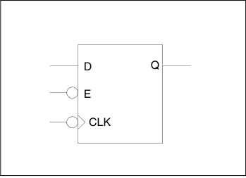
DFE1C_CC
This component is supported by ACT 2, ACT 3, 3200DX, MX, SX, SX-A, SX-S, eX families.
Figure 14-412. DFE1C_CC Logic Diagram
Function: D-Type Flip-Flop with active low Enable and Clock
Input: D, E, CLK
Output: Q
Table 14-726. Truth Table
E
CLK
Qn+1
1
X
Q
0
↓
D
Table 14-727. Modules
Family
Seq
Comb
ACT 2, ACT 3, 3200DX, MX
—
2
SX, SX-A, SX-S, eX
1
—
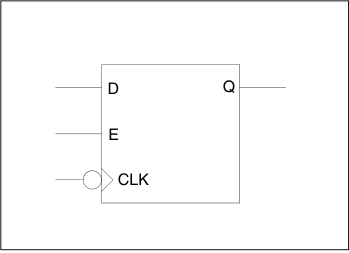
DFEA_CC
This component is supported by ACT 2, ACT 3, 3200DX, MX families.
Figure 14-413. DFEA_CC Logic Diagram
Function: D-Type Flip-Flop with Enable and active low Clock
Input: D, E, CLK
Output: Q
Table 14-728. Truth Table
E
CLK
Qn+1
0
X
Q
1
↓
D
Table 14-729. Modules
Family
Seq
Comb
ACT 2, ACT 3, 3200DX, MX
—
2
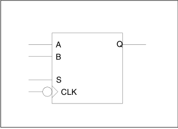
DFM_CC
This component is supported by ACT 2, ACT 3, 3200DX, MX families.
Figure 14-414. DFM_CC Logic Diagram
Function: D-Type Flip-Flop with 2-input Multiplexed Data
Input: A, B, S, CLK
Output: Q
Table 14-730. Truth Table
S
CLK
Qn+1
0
↑
A
1
↑
B
Table 14-731. Modules
Family
Seq
Comb
All listed
—
2
DFMA_CC
This component is supported by ACT 2, ACT 3, 3200DX, MX families.
Figure 14-415. DFMA_CC Logic Diagram
Function: D-Type Flip-Flop with 2-input Multiplexed Data and active low Clock
Input: A, B, S, CLK
Output: Q
Table 14-732. Truth Table
S
CLK
Qn+1
0
↓
A
1
↓
B
Table 14-733. Modules
Family
Seq
Comb
ACT 2, ACT 3, 3200DX, MX
—
2
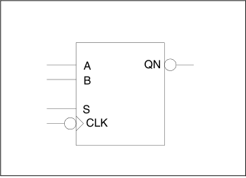
DFM1B_CC
This component is supported by ACT 2, ACT 3, 3200DX, MX families.
Figure 14-416. DFM1B_CC Logic Diagram
Function: D-Type Flip-Flop with 2-input Multiplexed Data and active low Output
Input: A, B, S, CLK
Output: QN
Table 14-734. Truth Table
S
CLK
QNn+1
0
↑
!A
1
↑
!B
Table 14-735. Modules
Family
Seq
Comb
All listed
—
2
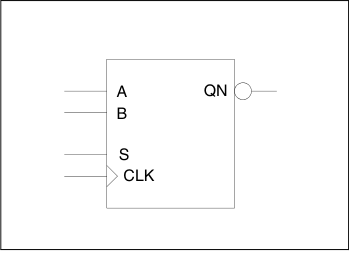
DFM1C_CC
This component is supported by ACT 2, ACT 3, 3200DX, MX families.
Figure 14-417. DFM1C_CC Logic Diagram
Function: D-Type Flip-Flop with 2-input Multiplexed Data and active low Clock and
Output
Input: A, B, S, CLK
Output: QN
Table 14-736. Truth Table
S
CLK
QNn+1
0
↓
!A
1
↓
!B
Table 14-737. Modules
Family
Seq
Comb
All listed
—
2
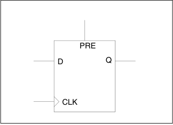
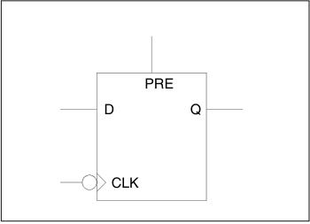
DFP1_CC*
This component is supported by ACT 2, ACT 3, 3200DX, MX, SX, SX-A, SX-S, eX families.
Figure 14-418. DFP1_CC Logic Diagram
Function: D-Type Flip-Flop with active high Preset
Input: D, PRE, CLK
Output: Q
Table 14-738. Truth Table
PRE
CLK
Qn+1
1
X
1
0
↑
D
Table 14-739. Modules
Family
Seq
Comb
ACT 2, ACT 3, 3200DX, MX
—
2
SX, SX-A, SX-S, eX
1
1
Note: Identical to macro DFP1.
DFP1A_CC*
This component is supported by ACT 2, ACT 3, 3200DX, MX, SX, SX-A, SX-S, eX families.
Figure 14-419. DFP1A_CC Logic Diagram
Function: D-Type Flip-Flop with active high Preset and active low Clock
Input: D, PRE, CLK
Output: Q
Table 14-740. Truth Table
PRE
CLK
Qn+1
1
X
1
0
↓
D
Table 14-741. Modules
Family
Seq
Comb
ACT 2, ACT 3, 3200DX, MX
—
2
SX, SX-A, SX-S, eX
1
1
Note: Identical to macro DFP1A.
DFP1B_CC*
This component is supported by ACT 2, ACT 3, 3200DX, MX, SX, SX-A, SX-S, eX, Accelerator
families.
Figure 14-420. DFP1B_CC Logic Diagram
Function: D-Type Flip-Flop with active low Preset
Input: D, PRE, CLK
Output: Q
Table 14-742. Truth Table
PRE
CLK
Qn+1
0
X
1
1
↑
D
Table 14-743. Modules
Family
Seq
Comb
All
—
2
Note: Identical to macro DFP1B.
DFP1D_CC*
This component is supported by ACT 2, ACT 3, 3200DX, MX, SX, SX-A, SX-S, eX families.
Figure 14-421. DFP1D_CC Logic Diagram
Function: D-Type Flip-Flop with active low Preset and Clock
Input: D, PRE, CLK
Output: Q
Table 14-744. Truth Table
PRE
CLK
Qn+1
0
X
1
1
↓
D
Table 14-745. Modules
Family
Seq
Comb
ACT 2, ACT 3, 3200DX, MX
—
2
SX, SX-A, SX-S, eX
1
—
Note: Identical to macro DFP1D.
DFPC_CC*
This component is supported by ACT 2, ACT 3, 3200DX, MX, SX, SX-A, SX-S, eX families.
Figure 14-422. DFPC_CC Logic Diagram
Function: D-Type Flip-Flop with active high Preset, active low Clear, and active high
Clock
Input: CLR, D, PRE, CLK
Output: Q
Table 14-746. Truth Table
CLR
PRE
CLK
Qn+1
0
X
X
0
1
1
X
1
1
0
↑
D
Table 14-747. Modules
Family
Seq
Comb
ACT 2, ACT 3, 3200DX, MX
—
2
SX, SX-A, SX-S, eX
1
1
Note: Identical to macro DFPC.
DFPCA_CC*
This component is supported by ACT 2, ACT 3, 3200DX, MX, SX, SX-A, SX-S, eX families.
Figure 14-423. DFPCA_CC Logic Diagram
Function: D-Type Flip-Flop with active high Preset, active low Clear, and active low
Clock
Input: CLR, D, PRE, CLK
Output: Q
Table 14-748. Truth Table
CLR
PRE
CLK
Qn+1
0
0
X
0
1
1
X
1
1
0
↓
D
0
1
X
**
Table 14-749. Modules
Family
Seq
Comb
ACT 2, ACT 3, 3200DX, MX
—
2
SX, SX-A, SX-S, eX
1
1
Note: Identical to macro DFPCA.
Note: Your design should not allow both PRE and CLR to be asserted at
the same time.