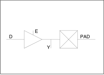
BIBUF This component is supported by ACT 1, ACT 2, ACT 3, 3200DX, MX, SX, SX-A, SX-S, eX, Accelerator families.
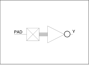
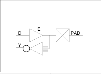
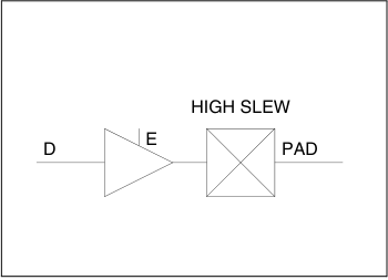
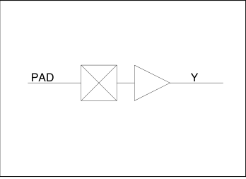
Figure 14-438. BIBUF Logic Diagram Function: Bidirectional Buffer, High Slew with Hidden Buffer at Y pin Input: D, E, PAD Output: PAD, Y Table 14-789. Truth Table MODE E D PAD Y OUTPUT 1 X D D INPUT 0 X X PAD
Table 14-790. Modules Family Seq I/O All — 1
CLKBIBUF This component is supported by ACT1, ACT2, ACT3, 3200DX, 42MX, 54SX, 54SX-A, Accelerator families.
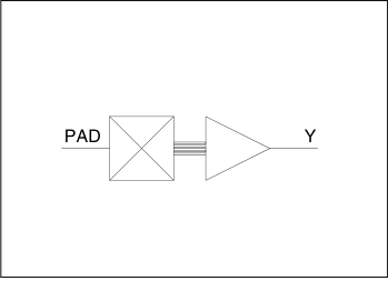
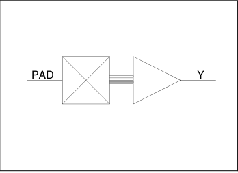
Figure 14-439. CLKBIBUF Logic Diagram Function: Bidirectional with input dedicated to hardwired clock network Input: D, E, PAD Output: PAD, Y Table 14-791. Truth Table D E PAD Y X 0 Z X X 0 0 0 X 0 1 1 0 1 0 0 1 1 1 1
Table 14-792. Modules Family Seq I/O All listed — 1
Note: Refer to the device-specific datasheet for more Clock Network information.
HCLKBIBUF This component is supported by ACT1, ACT2, ACT3, 3200DX, 42MX, 54SX, 54SX-A, Accelerator families.
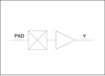
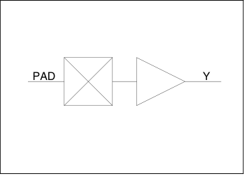
Figure 14-440. HCLKBIBUF Logic Diagram Function: Bidirectional with input dedicated to hardwired clock network. HCLKS hardwired clocks can drive only the CLK pins of the dedicated R-Cells, RAM Clock Pins Read and Write, and I/O-REG Clock Pins. The HCLKS cannot drive any other pins of R-Cells, or any pins of C-cells; this rules out CC-Flipflops as well. Input: D, E, PAD Output: PAD, Y Table 14-793. Truth Table D E PAD Y X 0 Z X X 0 0 0 X 0 1 1 0 1 0 0 1 1 1 1
Table 14-794. Modules Family Seq I/O All listed — 1
Note: Refer to the device-specific datasheet for more Clock Network information.
CLKBIBUFI This component is supported by SX-A, SX-S families.
Figure 14-441. CLKBIBUFI Logic Diagram Function: Bidirectional with inverted input dedicated to routed Clock Network. The CLKBIBUFI macro is intended for the SX72-A and SX72-S devices. Input: D, E, PAD Output: PAD, Y Table 14-795. Truth Table D E PAD Y X 0 Z X X 0 0 1 X 0 1 0 0 1 0 1 1 1 1 0
Table 14-796. Modules Family Seq I/O SX-A, SX-S — 1
Note: Refer to the device-specific datasheet for more Clock Network information.
CLKBUF This component is supported by ACT 1, ACT 2, ACT 3, 3200DX, MX, SX, SX-A, SX-S, eX, Accelerator families.
Figure 14-442. CLKBUF Logic Diagram Function: Input for Dedicated Routed Clock Network Input: PAD Output: Y Table 14-797. Truth Table PAD Y 0 0 1 1
Table 14-798. Modules Family Seq I/O All — 1
Note: NOTE 1: For an internal Clock net, refer to the CLKINT macro.
Note: NOTE 2: Refer to Microchip's Databook for more Clock Network information.
CLKBUFI This component is supported by SX, SX-A, SX-S, eX families.
Figure 14-443. CLKBUFI Logic Diagram Function: Inverting Input for Dedicated Routed Clock Network Input: PAD Output: Y Table 14-799. Truth Table PAD Y 0 1 1 0
Table 14-800. Modules Family Seq I/O SX, SX-A, SX-S, eX — 1
Note: NOTE 1: For an internal Clock net, refer to the CLKINTI macro.
Note: NOTE 2: Refer to Microchip's Databook for more Clock Network information.
HCLKBUF This component is supported by ACT 3, SX, SX-A, SX-S, eX, Accelerator families.
Figure 14-444. HCLKBUF Logic Diagram Function: Dedicated high-speed S-Module Clock Buffer Input: PAD Output: Y Table 14-801. Truth Table PAD Y 0 0 1 1
Table 14-802. Modules Family Seq I/O All listed — 1
Note: Refer to Microchip's Databook for more Clock Network information.
INBUF This component is supported by ACT 1, ACT 2, ACT 3, 3200DX, MX, SX, SX-A, SX-S, eX, Accelerator families.
Figure 14-445. INBUF Logic Diagram Function: Input Buffer Input: PAD Output: Y Table 14-803. Truth Table PAD Y 0 0 1 1
Table 14-804. Modules Family Seq I/O All listed — 1
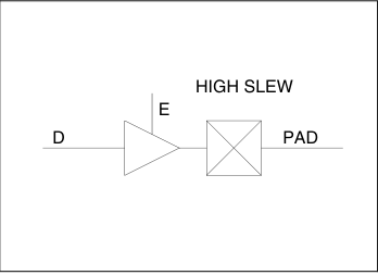
OUTBUF This component is supported by ACT 1, ACT 2, ACT 3, 3200DX, MX, SX, SX-A, SX-S, eX, Accelerator families.
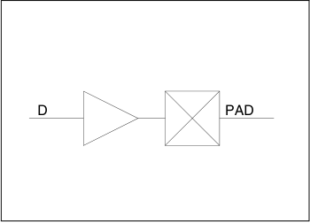
Figure 14-446. OUTBUF Logic Diagram Function: Output Buffer, High Slew Input: D Output: PAD Table 14-805. Truth Table D PAD 0 0 1 1
Table 14-806. Modules Family Seq I/O All — 1
QCLKBIBUFI
This component is supported by SX-A, SX-S families.
Figure 14-447. QCLKBIBUFI Logic Diagram Function: Bidirectional with inverted Input Dedicated to routed Clock Network. The QCLKBIBUFI macro is intended for the SX72-A and SX72-S devices. Input: D, E, PAD Output: PAD, Y Table 14-807. Truth Table D E PAD Y X 0 Z X X 0 0 1 X 0 1 0 0 1 0 1 1 1 1 0
Table 14-808. Modules Family Seq I/O SX-A, SX-S — 1
Note: Refer to Microchip's Databook for more Clock Network information.
QCLKBUF This component is supported by 3200DX, MX, SX-A, SX-S families.
Figure 14-448. QCLKBUF Logic Diagram Function: Input for Dedicated Routed Clock Network Input: PAD Output: Y Table 14-809. Truth Table PAD Y 0 0 1 1
Table 14-810. Modules Family Seq I/O All listed — 1
Note: NOTE 1: For an internal Clock net, refer to the CLKINT macro.
Note: NOTE 2: Refer to Microchip's Databook for more Clock Network information.
QCLKBUFI This component is supported by SX-A, SX-S families.
Figure 14-449. QCLKBUFI Logic Diagram Function: Inverted Input for Dedicated Routed Clock Network. The QCLKBUFI macro is intended for the SX72-A and SX72-S devices. Input: PAD Output: Y Table 14-811. Truth Table PAD Y 0 1 1 0
Table 14-812. Modules Family Seq I/O SX-A, SX-S — 1
Note: NOTE 1: For an internal Clock net, refer to the CLKINTI macro.
Note: NOTE 2: Refer to Microchip's Databook for more Clock Network information.
TRIBUFF This component is supported by ACT 1, ACT 2, ACT 3, 3200DX, MX, SX, SX-A, SX-S, eX families.
Figure 14-450. TRIBUFF Logic Diagram Function: Tristate Output, High Slew Input: D, E Output: PAD Table 14-813. Truth Table E PAD 0 Z 1 D
Table 14-814. Modules Family Seq I/O All — 1
Note: Refer to Microchip's Databook for internal tristate implementation using multiplexers.
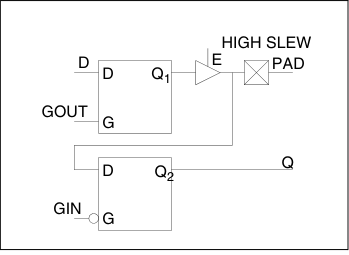
BBDLHS This component is supported by ACT 2, 3200DX, MX families.
Figure 14-451. BBDLHS Logic Diagram Function: Bidirectional with Input Latch and Output Latch Input: D, E, GOUT, GIN, PAD Output: PAD, Q Table 14-815. Truth Table MODE E GOUT GIN PAD Q OUTPUT 1 0 1 PADn-1 Qn-1 OUTPUT 1 1 0 D D INPUT 0 X 1 X Qn-1 INPUT 0 X 0 X PAD TRISTATE 0 X X Z X
Table 14-816. Modules Family Seq I/O All listed — 1
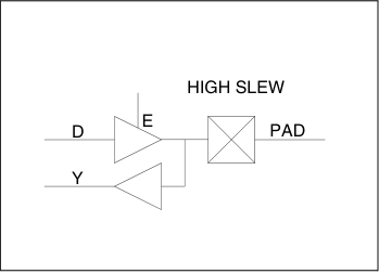
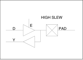
BBHS This component is supported by ACT 2, ACT 3, 3200DX, MX families.
Figure 14-452. BBHS Logic Diagram Function: Bidirectional Buffer, High Slew Input: D, E, PAD Output: PAD, Y Table 14-817. Truth Table MODE E PAD Y OUTPUT 1 D D INPUT 0 X PAD
Table 14-818. Modules Family Seq I/O All listed — 1
Note: For new designs, instead of BBHS we recommend that you use BIBUF.
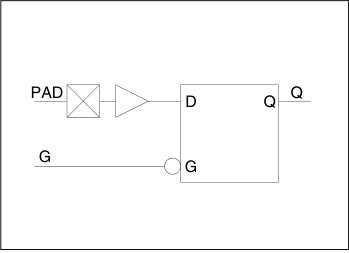
IBDL This component is supported by ACT 2, 3200DX, MX families.
Figure 14-453. IBDL Logic Diagram Function: Input Buffer with Input Latch, with active low Clock Input: G, PAD Output: Q Table 14-819. Truth Table G Q 1 Qn-1 0 PAD
Table 14-820. Modules Family Seq I/O All listed — 1
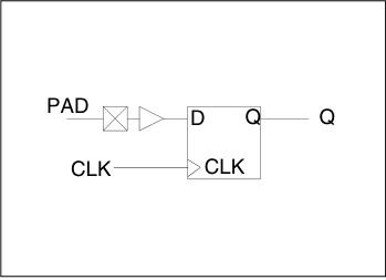
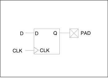
IR This component is supported by ACT 2, 3200DX, MX families.
Figure 14-454. IR Logic Diagram Function: Input Register Input: PAD, CLK Output: Q Table 14-821. Truth Table CLK Q ↑ PAD
Table 14-822. Modules Family Seq I/O All listed 1 1
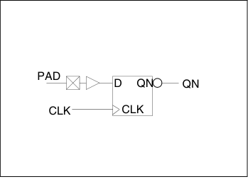
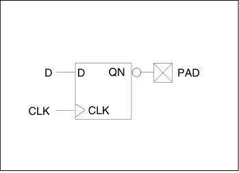
IRI This component is supported by ACT 2, 3200DX, MX families.
Figure 14-455. IRI Logic Diagram Function: Input register with active Low output Input: PAD, CLK Output: QN Table 14-823. Truth Table CLK QN ↑ !PAD
Table 14-824. Modules Family Seq I/O All listed 1 1
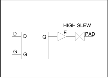
OBDLHS This component is supported by ACT 2, 3200DX, MX families.
Figure 14-456. OBDLHS Logic Diagram Function: Output Buffer with Output Latch, High Slew Input: D, G Output: PAD Table 14-825. Truth Table G PAD 0 PADn-1 1 D
Table 14-826. Modules Family Seq I/O All listed — 1
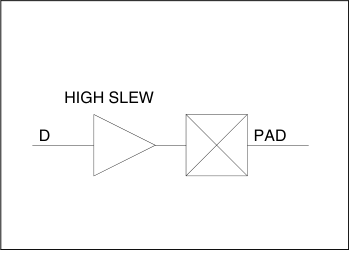
OBHS This component is supported by ACT 2, ACT 3, 3200DX, MX families.
Figure 14-457. OBHS Logic Diagram Function: Output Buffer, High Slew Input: D Output: PAD Table 14-827. Truth Table D PAD 0 0 1 1
Table 14-828. Modules Family Seq I/O All listed — 1
Note: For new designs, instead of OBHS we recommend that you use OUTBUF.
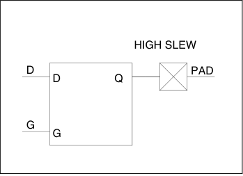
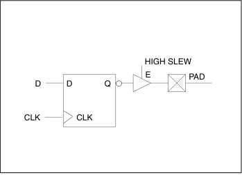
ORH This component is supported by ACT 2, 3200DX, MX families.
Figure 14-458. ORH Logic Diagram Function: Output Register, High Slew Input: D, CLK Output: PAD Table 14-829. Truth Table CLK PADn+1 ↑ D
Table 14-830. Modules Family Seq I/O All listed 1 1
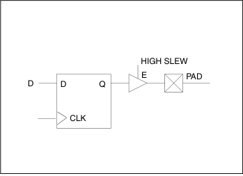
ORIH This component is supported by ACT 2, 3200DX, MX families.
Figure 14-459. ORIH Logic Diagram Function: Inverted Output Register, High Slew Input: D, CLK Output: PAD Table 14-831. Truth Table CLK PADn+1 ↑ !D
Table 14-832. Modules Family Seq I/O All listed 1 1
This component is supported by ACT 2, 3200DX, MX families.
Figure 14-460. ORITH Logic Diagram Function: Inverted Output Register, Tristate Enable, High Slew Input: D, E, CLK Output: PAD Table 14-833. Truth Table E CLK PADn+1 0 X Z 1 ↑ !D
Table 14-834. Modules Family Seq I/O All listed 1 1
ORTH This component is supported by ACT 2, 3200DX, MX families.
Figure 14-461. ORTH Logic Diagram Function: Output Register, Tristate Enable, High Slew Input: D, E, CLK Output: PAD Table 14-835. Truth Table E CLK PADn+1 0 X Z 1 ↑ D
Table 14-836. Modules Family Seq I/O All listed 1 1
TBDLHS This component is supported by ACT 2, 3200DX, MX families.
Figure 14-462. TBDLHS Logic Diagram Function: Tristate Output with Latch, High Slew Input: D, E, G Output: PAD Table 14-837. Truth Table E G PAD 0 X Z 1 1 D 1 0 PADn-1
Table 14-838. Modules Family Seq I/O All listed — 1
TBHS This component is supported by ACT 2, ACT 3, 3200DX, MX families.
Figure 14-463. TBHS Logic Diagram Function: Tristate Output, High Slew Input: D, E Output: PAD Table 14-839. Truth Table E PAD 0 Z 1 D
Table 14-840. Modules Family Seq I/O All listed — 1
Note: For new designs, instead of TBHS we recommend that you use TRIBUFF.
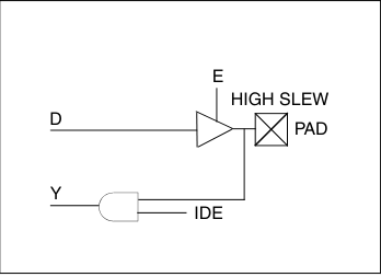
BBHSA This component is supported by ACT 3 family.
Figure 14-464. BBHSA Logic Diagram Function: Bidirectional buffer with AND gate, High Slew Input: D, E, IDE, PAD Output: PAD, Y Table 14-841. Truth Table MODE E IDE PAD Y OUTPUT 1 1 D D OUTPUT 1 0 D 0 INPUT 0 1 X PAD INPUT 0 0 X 0
Table 14-842. Modules Family Seq I/O ACT 3 — 1
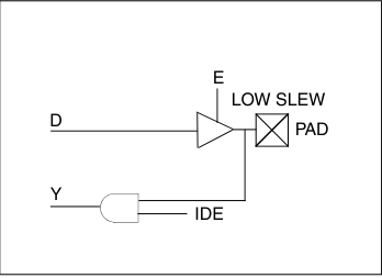
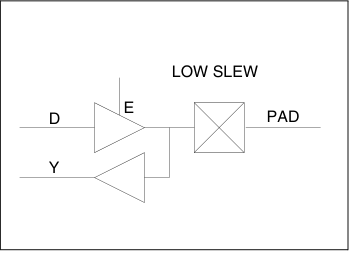
BBLSA This component is supported by ACT 3 family.
Figure 14-465. BBLSA Logic Diagram Function: Bidirectional buffer with AND gate, Low Slew Input: D, E, IDE, PAD Output: PAD, Y Table 14-843. Truth Table MODE E IDE PAD Y OUTPUT 1 1 D D OUTPUT 1 0 D 0 INPUT 0 1 X PAD INPUT 0 0 X 0
Table 14-844. Modules Family Seq I/O ACT 3 — 1
BBUFTH This component is supported by ACT 3 family.
Figure 14-466. BBUFTH Logic Diagram Function: Bidirectional Buffer, Tristate Enable, High Slew Input: D, E, PAD Output: PAD, Y Table 14-845. Truth Table MODE E PAD Y OUTPUT 1 D D INPUT 0 X PAD
Table 14-846. Modules Family Seq I/O ACT 3 — 1
BBUFTL Logic Diagram Function: Bidirectional Buffer, Tristate Enable, Low Slew Input: D, E, PAD Output: PAD, Y Table 14-847. Truth Table MODE E PAD Y OUTPUT 1 D D INPUT 0 X PAD
Table 14-848. Modules Family Seq I/O ACT 3 — 1
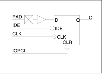
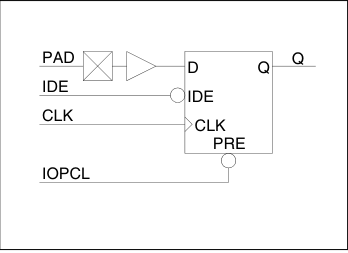
BIECTH This component is supported by ACT 3 family.
Figure 14-467. BIECTH Logic Diagram Function: Bidirectional Input Register with Clear, Input Data Enable, Tristate Enable, High Slew Input: D, E, IDE, CLK, IOPCL, PAD Output: PAD, Q Table 14-849. Truth Table MODE E IOPCL IDE CLK PAD Q OUTPUT 1 0 X X D 0 OUTPUT 1 1 0 ↑ D D OUTPUT 1 1 1 ↑ D Qn-1 INPUT 0 0 X X X 0 INPUT 0 1 0 ↑ X PAD INPUT 0 1 1 ↑ X Qn-1
Table 14-850. Modules Family Seq I/O ACT 3 — 1
BIECTL This component is supported by ACT 3 family.
Figure 14-468. BIECTL Logic Diagram Function: Bidirectional Input Register with Clear, Input Data Enable, Tristate Enable, Low Slew Input: D, E, IDE, CLK, IOPCL, PAD Output: PAD, Q Table 14-851. Truth Table MODE E IOPCL IDE CLK PAD Q OUTPUT 1 0 X X D 0 OUTPUT 1 1 0 ↑ D D OUTPUT 1 1 1 ↑ D Qn-1 INPUT 0 0 X X X 0 INPUT 0 1 0 ↑ X PAD INPUT 0 1 1 ↑ X Qn-1
Table 14-852. Modules Family Seq I/O ACT 3 — 1
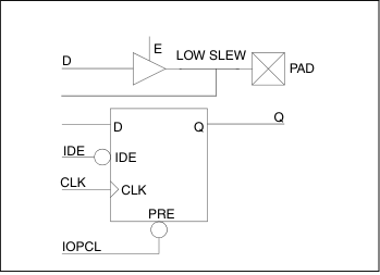
BIEPTH This component is supported by ACT 3 family.
Figure 14-469. BIEPTH Logic Diagram Function: Bidirectional Input Register with Preset, Input Data Enable, Tristate Enable, High Slew Input: D, E, IDE, CLK, IOPCL, PAD Output: PAD, Q Table 14-853. Truth Table MODE E IOPCL IDE CLK PAD Q OUTPUT 1 0 X X D 1 OUTPUT 1 1 0 ↑ D D OUTPUT 1 1 1 ↑ D Qn-1 INPUT 0 0 X X X 1 INPUT 0 1 0 ↑ X PAD INPUT 0 1 1 ↑ X Qn-1
Table 14-854. Modules Family Seq I/O ACT 3 — 1
BIEPTL This component is supported by ACT 3 family.
Figure 14-470. BIEPTL Logic Diagram Function: Bidirectional Input Register with Preset, Input Data Enable, Tristate Enable, Low Slew Input: D, E, IDE, CLK, IOPCL, PAD Output: PAD, Q Table 14-855. Truth Table MODE E IOPCL IDE CLK PAD Q OUTPUT 1 0 X X D 1 OUTPUT 1 1 0 ↑ D D OUTPUT 1 1 1 ↑ D Qn-1 INPUT 0 0 X X X 1 INPUT 0 1 0 ↑ X PAD INPUT 0 1 1 ↑ X Qn-1
Table 14-856. Modules Family Seq I/O ACT 3 — 1
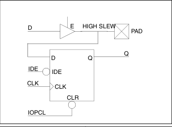
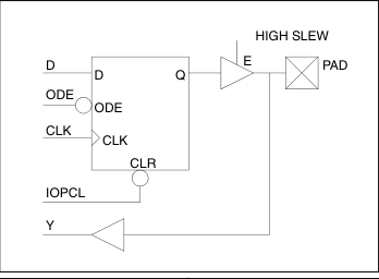
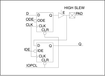
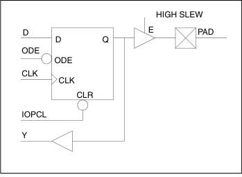
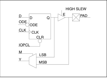
BRECTH This component is supported by ACT 3 family.
Figure 14-471. BRECTH Logic Diagram Function: Bidirectional Output Register, with Clear, Output Data Enable, Tristate Enable, High Slew Input: D, E, ODE, CLK, IOPCL, PAD Output: PAD, Y Table 14-857. Truth Table MODE E IOPCL ODE CLK PAD Y OUTPUT 1 0 X X 0 0 OUTPUT 1 1 1 ↑ PADn-1 Yn-1 OUTPUT 1 1 0 ↑ D D INPUT 0 X X X X PAD
Table 14-858. Modules Family Seq I/O ACT 3 — 1
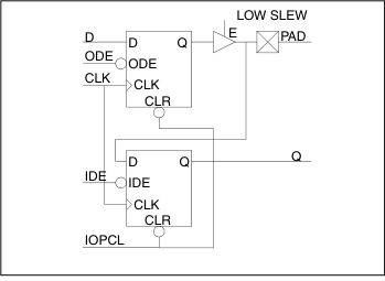
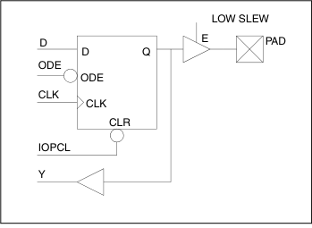
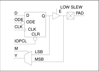
BRECTL This component is supported by ACT 3 family.
Figure 14-472. BRECTL Logic Diagram Function: Bidirectional Output Register, with Clear, Output Data Enable, Tristate Enable, Low Slew Input: D, E, ODE, CLK, IOPCL, PAD Output: PAD, Y Table 14-859. Truth Table MODE E IOPCL ODE CLK PAD Y OUTPUT 1 0 X X 0 0 OUTPUT 1 1 1 ↑ PADn-1 Yn-1 OUTPUT 1 1 0 ↑ D D INPUT 0 X X X X PAD
Table 14-860. Modules Family Seq I/O ACT 3 — 1
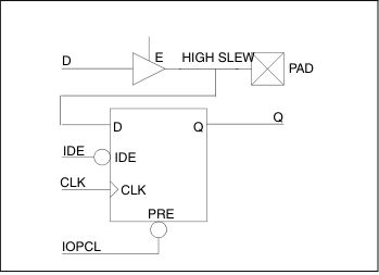
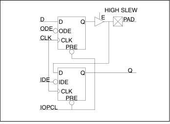
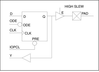
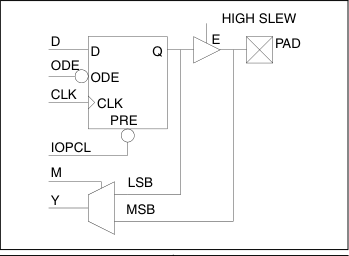
BREPTH This component is supported by ACT 3 family.
Figure 14-473. BREPTH Logic Diagram Function: Bidirectional Output Register, with Preset, Output Data Enable, Tristate Enable, High Slew Input: D, E, ODE, CLK, IOPCL, PAD Output: PAD, Y Table 14-861. Truth Table MODE E IOPCL ODE CLK PAD Y OUTPUT 1 0 X X 1 1 OUTPUT 1 1 1 ↑ PADn-1 Yn-1 OUTPUT 1 1 0 ↑ D D INPUT 0 X X X X PAD
Table 14-862. Modules Family Seq I/O ACT 3 — 1
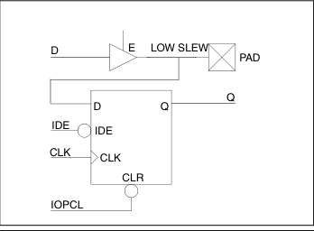
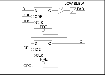
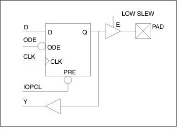
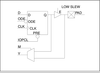
BREPTL This component is supported by ACT 3 family.
Figure 14-474. BREPTL Logic Diagram Function: Bidirectional Output Register, with Preset, Output Data Enable, Tristate Enable, Low Slew Input: D, E, ODE, CLK, IOPCL, PAD Output: PAD, Y Table 14-863. Truth Table MODE E IOPCL ODE CLK PAD Y OUTPUT 1 0 X X 1 1 OUTPUT 1 1 1 ↑ PADn-1 Yn-1 OUTPUT 1 1 0 ↑ D D INPUT 0 X X X X PAD
Table 14-864. Modules Family Seq I/O ACT 3 — 1
DECETH This component is supported by ACT 3 family.
Figure 14-475. DECETH Logic Diagram Function: Bidirectional Double Registered, with Clear, Input Data Enable, Tristate Enable, High Slew, Output Data Enable Input: D, E, ODE, CLK, IOPCL, IDE, PAD Output: PAD, Q Table 14-865. Truth Table MODE E IOPCL ODE IDE CLK PAD Q OUTPUT 1 0 X X X 0 0 OUTPUT 1 1 0 0 ↑ D PAD OUTPUT 1 1 1 1 X PADn-1 Qn-1 INPUT 0 0 X X X X 0 INPUT 0 1 X 0 ↑ X PAD INPUT 0 1 X 1 X X Qn-1
Table 14-866. Modules Family Seq I/O ACT 3 — 1
DECETL This component is supported by ACT 3 family.
Figure 14-476. DECETL Logic Diagram Function: Bidirectional Double Registered, with Clear, Input Data Enable, Tristate Enable, Low Slew, Output Data Enable Input: D, E, ODE, CLK, IOPCL, IDE, PAD Output: PAD, Q Table 14-867. Truth Table MODE E IOPCL ODE IDE CLK PAD Q OUTPUT 1 0 X X X 0 0 OUTPUT 1 1 0 0 ↑ D PAD OUTPUT 1 1 1 1 X PADn-1 Qn-1 INPUT 0 0 X X X X 0 INPUT 0 1 X 0 ↑ X PAD INPUT 0 1 X 1 X X Qn-1
Table 14-868. Modules Family Seq I/O ACT 3 — 1
DEPETH This component is supported by ACT 3 family.
Figure 14-477. DEPETH Logic Diagram Function: Bidirectional Double Registered, with Preset, Input Data Enable, Tristate Enable, High Slew, Output Data Enable Input: D, E, ODE, CLK, IOPCL, IDE, PAD Output: PAD, Q Table 14-869. Truth Table MODE E IOPCL ODE IDE CLK PAD Q OUTPUT 1 0 X X X 1 1 OUTPUT 1 1 0 0 ↑ D PAD OUTPUT 1 1 1 1 X PADn-1 Qn-1 INPUT 0 0 X X X X 1 INPUT 0 1 X 0 ↑ X PAD INPUT 0 1 X 1 X X Qn-1
Table 14-870. Modules Family Seq I/O ACT 3 — 1
DEPETL This component is supported by ACT 3 family.
Figure 14-478. DEPETL Logic Diagram Function: Bidirectional Double Registered, with Preset, Input Data Enable, Tristate Enable, Low Slew, Output Data Enable Input: D, E, ODE, CLK, IOPCL, IDE, PAD Output: PAD, Q Table 14-871. Truth Table MODE E IOPCL ODE IDE CLK PAD Q OUTPUT 1 0 X X X 1 1 OUTPUT 1 1 0 0 ↑ D PAD OUTPUT 1 1 1 1 X PADn-1 Qn-1 INPUT 0 0 X X X X 1 INPUT 0 1 X 0 ↑ X PAD INPUT 0 1 X 1 X X Qn-1
Table 14-872. Modules Family Seq I/O ACT 3 — 1
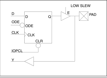
FECTH This component is supported by ACT 3 family.
Figure 14-479. FECTH Logic Diagram Function: Output Register with feedback, Clear, Output Data Enable, Tristate Enable, High Slew Input: D, E, ODE, CLK, IOPCL, PAD Output: PAD, Y Table 14-873. Truth Table E IOPCL ODE CLK Y PAD 1 0 X X 0 0 1 1 0 ↑ D D 1 1 1 X Yn-1 PADn-1 0 0 X X 0 Z 0 1 0 ↑ D Z 0 1 1 X Yn-1 Z
Table 14-874. Modules Family Seq I/O ACT 3 — 1
FECTL This component is supported by ACT 3 family.
Figure 14-480. FECTL Logic Diagram Function: Output Register with feedback, Clear, Output Data Enable, Tristate Enable, Low Slew Input: D, E, ODE, CLK, IOPCL, PAD Output: PAD, Y Table 14-875. Truth Table E IOPCL ODE CLK Y PAD 1 0 X X 0 0 1 1 0 ↑ D D 1 1 1 X Yn-1 PADn-1 0 0 X X 0 Z 0 1 0 ↑ D Z 0 1 1 X Yn-1 Z
Table 14-876. Modules Family Seq I/O ACT 3 — 1
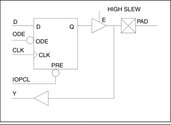
FEPTH This component is supported by ACT 3 family.
Figure 14-481. FEPTH Logic Diagram Function: Output Register with feedback, Preset, Output Data Enable, Tristate Enable, High Slew Input: D, E, ODE, CLK, IOPCL, PAD Output: PAD, Y Table 14-877. Truth Table E IOPCL ODE CLK Y PAD 1 0 X X 1 1 1 1 0 ↑ D D 1 1 1 X Yn-1 PADn-1 0 0 X X 1 Z 0 1 0 ↑ D Z 0 1 1 X Yn-1 Z
Table 14-878. Modules Family Seq I/O ACT 3 — 1
FEPTL This component is supported by ACT 3 family.
Figure 14-482. FEPTL Logic Diagram Function: Output Register with feedback, Preset, Output Data Enable, Tristate Enable, Low Slew Input: D, E, ODE, CLK, IOPCL, PAD Output: PAD, Y Table 14-879. Truth Table E IOPCL ODE CLK Y PAD 1 0 X X 1 1 1 1 0 ↑ D D 1 1 1 X Yn-1 PADn-1 0 0 X X 1 Z 0 1 0 ↑ D Z 0 1 1 X Yn-1 Z
Table 14-880. Modules Family Seq I/O ACT 3 — 1
FECTMH This component is supported by ACT 3 family.
Figure 14-483. FECTMH Logic Diagram Function: Output Register with Muxed Feedback, Clear, Output Data Enable, Tristate Enable, High Slew Input: D, E, ODE, CLK, IOPCL, PAD, M Output: PAD, Y Table 14-881. Truth Table MODE E IOPCL ODE CLK PAD M Y OUTPUT 1 0 X X 0 X 0 OUTPUT 1 1 0 ↑ D X D OUTPUT 1 1 1 X PADn-1 X Yn-1 INPUT 0 1 0 ↑ X 0 D INPUT 0 1 X X X 1 PAD
Table 14-882. Modules Family Seq I/O ACT 3 — 1
Note: When M = 0, LSB is selected. When M = 1, MSB is selected.
FECTML This component is supported by ACT 3 family.
Figure 14-484. FECTML Logic Diagram Function: Output Register with Muxed Feedback, Clear, Output Data Enable, Tristate Enable, Low Slew Input: D, E, ODE, CLK, IOPCL, PAD, M Output: PAD, Y Table 14-883. Truth Table MODE E IOPCL ODE CLK PAD M Y OUTPUT 1 0 X X 0 X 0 OUTPUT 1 1 0 ↑ D X D OUTPUT 1 1 1 X PADn-1 X Yn-1 INPUT 0 1 0 ↑ X 0 D INPUT 0 1 X X X 1 PAD
Table 14-884. Modules Family Seq I/O ACT 3 — 1
Note: When M = 0, LSB is selected. When M = 1, MSB is selected.
FEPTMH This component is supported by ACT 3 family.
Figure 14-485. FEPTMH Logic Diagram Function: Output Register with Muxed Feedback, Preset, Output Data Enable, Tristate Enable, High Slew Input: D, E, ODE, CLK, IOPCL, PAD, M Output: PAD, Y Table 14-885. Truth Table 1 MODE E IOPCL ODE CLK PAD M Y OUTPUT 1 0 X X 1 X 1 OUTPUT 1 1 0 ↑ D X D OUTPUT 1 1 1 X PADn-1 X Yn-1 INPUT 0 1 0 ↑ X 0 D INPUT 0 1 X X X 1 PAD
Note: When M = 0, LSB is selected. When M = 1, MSB is selected.
Table 14-886. Modules Family Seq I/O ACT 3 — 1
Note: When M = 0, LSB is selected. When M = 1, MSB is selected.
FEPTML This component is supported by ACT 3 family.
Figure 14-486. FEPTML Logic Diagram Function: Output Register with Muxed Feedback, Preset, Output Data Enable, Tristate Enable, Low Slew Input: D, E, ODE, CLK, IOPCL, PAD, M Output: PAD, Y Table 14-887. Truth Table 1 MODE E IOPCL ODE CLK PAD M Y OUTPUT 1 0 X X 1 X 1 OUTPUT 1 1 0 ↑ D X D OUTPUT 1 1 1 X PADn-1 X Yn-1 INPUT 0 1 0 ↑ X 0 D INPUT 0 1 X X X 1 PAD
Note: When M = 0, LSB is selected. When M = 1, MSB is selected.
Table 14-888. Modules Family Seq I/O ACT 3 — 1
Note: When M = 0, LSB is selected. When M = 1, MSB is selected.
IBUF This component is supported by ACT 3 family.
Figure 14-487. IBUF Logic Diagram Function: Input Buffer Input: PAD Output: Y Table 14-889. Truth Table PAD Y 0 0 1 1
Table 14-890. Modules Family Seq I/O ACT 3 — 1
IOCLKBUF This component is supported by ACT 3 family.
Figure 14-488. IOCLKBUF Logic Diagram Function: Dedicated I/O Module Clock Buffer Input: PAD Output: Y Table 14-891. Truth Table PAD Y 0 0 1 1
Table 14-892. Modules Family Seq I/O ACT 3 — 1
Note: Refer to Microchip’s Databook for more Clock Network information.
IOPCLBUF This component is supported by ACT 3 family.
Figure 14-489. IOPCLBUF Logic Diagram Function: Dedicated I/O Preset Clear Buffer Input: PAD Output: Y Table 14-893. Truth Table PAD Y 0 0 1 1
Table 14-894. Modules Family Seq I/O ACT 3 — 1
Note: Refer to Microchip’s Databook for more Clock Network information.
IREC This component is supported by ACT 3 family.
Figure 14-490. IREC Logic Diagram Function: Input Register, with Clear, Input Data Enable Input: PAD, IDE, CLK, IOPCL Output: Q Table 14-895. Truth Table IOPCL IDE CLK Qn+1 0 X X 0 1 1 X Q 1 0 ↑ PAD
Table 14-896. Modules Family Seq I/O ACT 3 — 1
IREP This component is supported by ACT 3 family.
Figure 14-491. IREP Logic Diagram Function: Input Register, with Preset, Input Data Enable Input: PAD, IDE, CLK, IOPCL Output: Q Table 14-897. Truth Table IOPCL IDE CLK Qn+1 0 X X 1 1 1 X Q 1 0 ↑ PAD
Table 14-898. Modules Family Seq I/O ACT 3 — 1
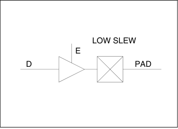
OBUFTH This component is supported by ACT 3 family.
Figure 14-492. OBUFTH Logic Diagram Function: Output Buffer, Tristate Enable, High Slew Input: D, E Output: PAD Table 14-899. Truth Table D E PAD X 0 Z 0 1 0 1 1 1
Table 14-900. Modules Family Seq I/O ACT 3 — 1
OBUFTL This component is supported by ACT 3 family.
Figure 14-493. OBUFTL Logic Diagram Function: Output Buffer, Tristate Enable, Low Slew Input: D, E Output: PAD Table 14-901. Truth Table D E PAD X 0 Z 0 1 0 1 1 1
Table 14-902. Modules Family Seq I/O ACT 3 — 1
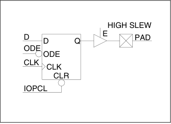
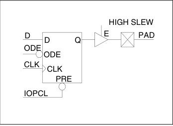
ORECTH This component is supported by ACT 3 family.
Figure 14-494. ORECTH Logic Diagram Function: Output Register, with Clear, Output Data Enable, Tristate Enable, High Slew Input: D, ODE, CLK, IOPCL, E Output: PAD Table 14-903. Truth Table IOPCL E ODE CLK PAD 0 1 X X 0 X 0 X X Z 1 1 0 ↑ D
Table 14-904. Modules Family Seq I/O ACT 3 — 1
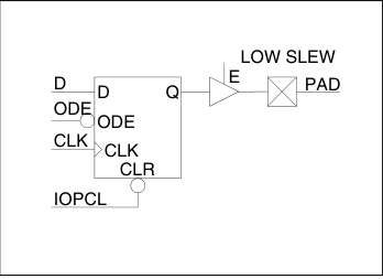
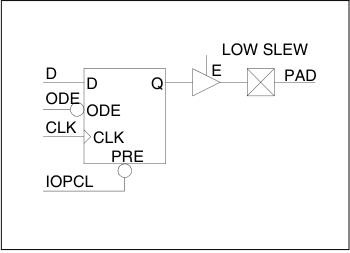
ORECTL This component is supported by ACT 3 family.
Figure 14-495. ORECTL Logic Diagram Function: Output Register, with Clear, Output Data Enable, Tristate Enable, Low Slew Input: D, ODE, CLK, IOPCL, E Output: PAD Table 14-905. Truth Table IOPCL E ODE CLK PAD 0 1 X X 0 X 0 X X Z 1 1 0 ↑ D
Table 14-906. Modules Family Seq I/O ACT 3 — 1
OREPTH This component is supported by ACT 3 family.
Figure 14-496. OREPTH Logic Diagram Function: Output Register, with Preset, Output Data Enable, Tristate Enable, High Slew Input: D, ODE, CLK, IOPCL, E Output: PAD Table 14-907. Truth Table IOPCL E ODE CLK PAD 0 1 X X 1 X 0 X X Z 1 1 0 ↑ D
Table 14-908. Modules Family Seq I/O ACT 3 — 1
OREPTL This component is supported by ACT 3 family.
Figure 14-497. OREPTL Logic Diagram Function: Output Register, with Preset, Output Data Enable, Tristate Enable, Low Slew Input: D, ODE, CLK, IOPCL, E Output: PAD Table 14-909. Truth Table IOPCL E ODE CLK PAD 0 1 X X 1 X 0 X X Z 1 1 0 ↑ D
Table 14-910. Modules Family Seq I/O ACT 3 — 1