
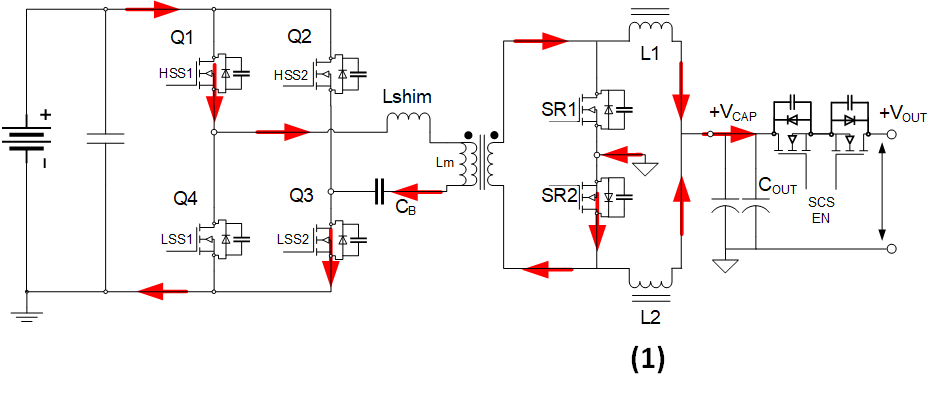
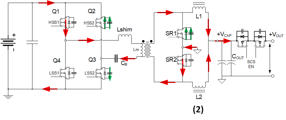
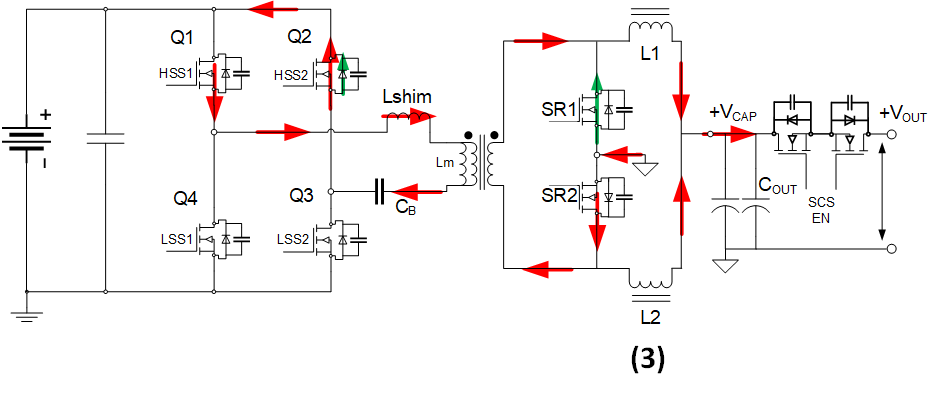
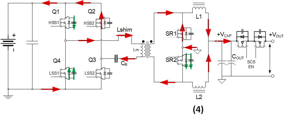
5.7 Synchronous Rectifiers
The system works naturally with Asynchronous rectification through the body diodes of the Rectification MOSFET (SR1, SR2). At a higher current, this produces losses due to a forward drop of the body diode, reducing efficiency and limiting maximum current transfer due to cooling required.
The following examples show how the SR MOSFETs SR1 and SR2 are switched.
|
|
|
|
|
|
|
|
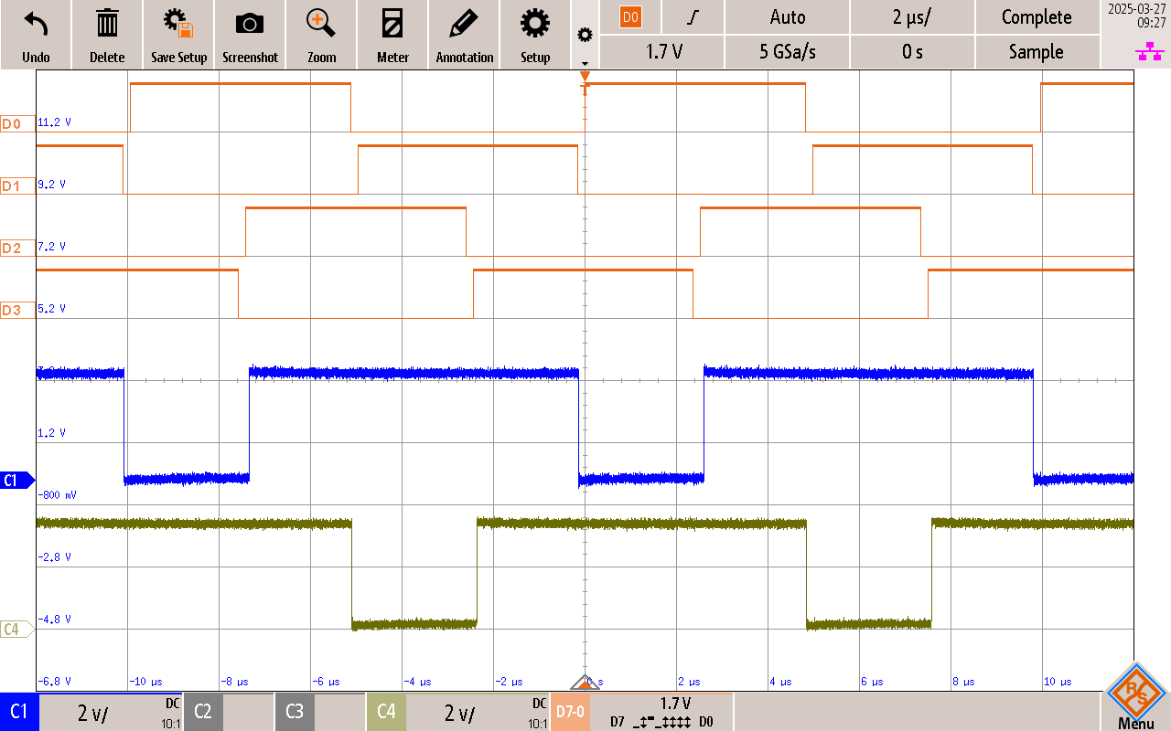 Channel details: Channel 1: SR1 CTRL Signal Channel 4: SR2 CTRL Signal Digital CH-0: D0 control for HSS1 Digital Ch-1: D1 control for LSS1 Digital CH-2: D2 control for HSS2 Digital CH-3: D3 control for LSS2 |
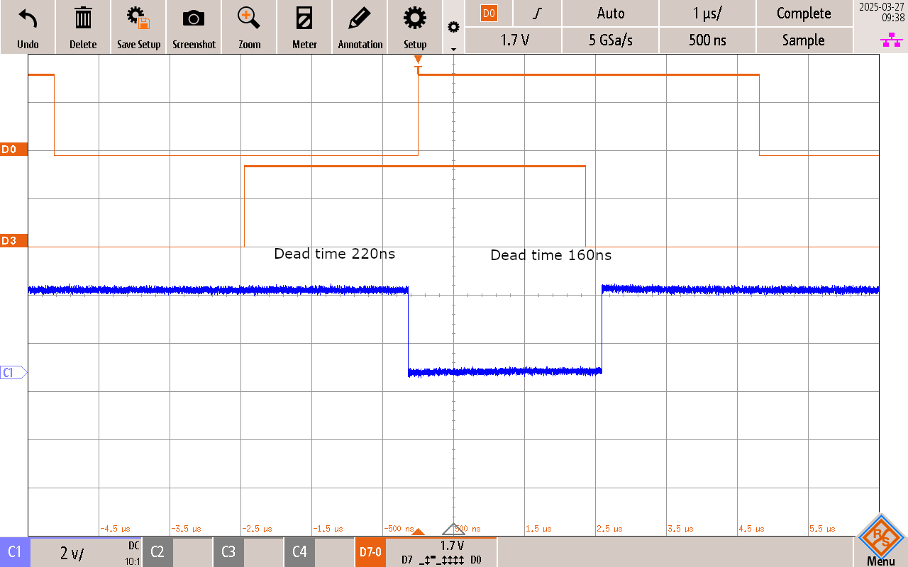 Channel details: Channel 1: SR1 CTRL Signal Channel 4: SR2 CTRL Signal Digital Ch-0: D0 control for HSS1 Digital Ch-3: D3 control for LSS2 |
Test conditions: VIN = 800V, VOUT = 15V, IOUT = 180A, Po = 2700W Channel details: Channel 1: SR gate-source voltage Channel 2: Transformer primary current Channel 3: Transformer primary voltage Channel 4: SR drain-source voltage |
SR Switching ON
Commutation of PSFB-CDR from phase 1 to 4 shows that SR1 goes from not conducting and turned OFF to fully ON and conducting in phase 4. In phase 1, SR1 Vds is equal to VIN/N (Turns ratio) of the transformer. In phase 2, the voltage applied to transformer primary reduces from VIN and swings to 0V. This results in drain-source voltage of SR1 to also reduce to 0V. At this point, SR1 is switched ON and turns on with full ZVS.
SR Switching OFF
Analyse SR2 as it switches from ON and fully conducting to switched OFF. SR2 is switched OFF from phase 3 to 4. In phase 3, SR2 is conducting approximately output current. SR2 is switched OFF right before phase 4, at which point SR2 MOSFET channel stops conducting and its body diode hits reverse recovery from the increased Vds and becomes reverse biased. Both SRs turn OFF with ZVS but still have body diode conduction losses due to dead time and reverse recovery losses.