
5.2 Primary Side Phase-Shifted Full-Bridge
The Primary Side Phase-Shifted Full-Bridge (PSFB) has two half-bridge legs. Each operates at 50% duty cycle. For this reference design, the operating frequency is 100 kHz with a dead time of 160 ns. The transformer is connected across both legs. The PSFB works by introducing a phase shift between the two legs. With the phase shift and dead time of 160 ns between high-side and low-side MOSFETs, a scheme supporting Zero Voltage Switching arises.
The commutation phases are explained in detail in Phase-Shifted Full-Bridge with Current Doubler Rectifier.
A closer observation shows that on the PSFB side, one leg is completely soft switched while the other leg runs in partial/low ZVS or full ZVS depending on the peak current on the primary side.
The peak current in Steady State conditions changes based on the following
- Input Voltage: A lower input voltage at the same output power will result in a higher primary side peak current.
- Output Voltage: Increasing output voltage increases duty and primary side transformer current increases to a higher value, resulting in higher ZVS.
- Output current or power: Higher output current results in higher transformer primary side peak current. This improves ZVS.
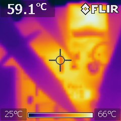
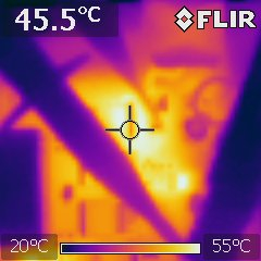
Test conditions: VIN=800V, VOUT = 12V, IOUT = 50A, Po = 600W Channel details: Channel 1: N/A Channel 2: Transformer primary side current Channel 3: Transformer primary side differential voltage Channel 4: N/A |
Test conditions: VIN = 800V, VOUT = 12V, IOUT = 100A, Po = 1200W Channel details: Channel 1: N/A Channel 2: Transformer primary side current Channel 3: Transformer primary side differential voltage Channel 4: N/A |
Test conditions: VIN = 800V, VOUT = 12V, IOUT = 150A, Po = 1800W Channel details: Channel 1: N/A Channel 2: Transformer primary side current Channel 3: Transformer primary side differential voltage Channel 4: N/A |
Test conditions: VIN = 800V, VOUT = 15V, IOUT = 180A, Po = 2700W Channel details: Channel 1: N/A Channel 2: Transformer primary side current Channel 3: Transformer primary side differential voltage Channel 4: N/A |
Test conditions: VIN = 800V, VOUT = 12V, IOUT=90A, Po = 1080W Channel details: Channel 1: N/A Channel 2: N/A Channel 3: PSFB Leg-1 Switch-node voltage Channel 4: PSFB Leg-1 HSS (High-Side Switch) Gate-source voltage |
Test conditions: VIN = 800V, VOUT = 12V, IOUT = 140A, Po = 1680W Channel details: Channel 1: N/A Channel 2: N/A Channel 3: PSFB Leg-1 Switch-node voltage Channel 4: PSFB Leg-1 HSS (High-Side Switch) Gate-source voltage |
Test conditions: VIN = 800V, VOUT = 15V, IOUT = 160A, Po = 2400W Channel details: Channel 1: N/A Channel 2: N/A Channel 3: PSFB Leg-1 Switch-node voltage Channel 4: PSFB Leg-1 HSS (High-Side Switch) Gate-source voltage |
 |
 |
Test conditions: VIN = 800V, VOUT = 12V, IOUT = 90A, Po = 1080W Observations: Lower peak currents in the PSFB primary side lead to lower conduction losses and results in lower leakage energy. This leads to partial ZVS resulting in higher switching losses. Lower conduction losses and higher switching losses due to partial ZVS. | Test conditions: VIN = 800V, VOUT = 12V, IOUT = 140A, Po = 1680W Observations: Higher peak current in the PSFB primary side leads to higher leakage energy stored. This energy is converted into voltage swing to charge/discharge PSFB MOSFET Coss. Higher conduction losses and lower switching losses due to Higher ZVS. |
Test conditions: VIN = 800V, VOUT = 12V, IOUT = 50A, Po = 600W Channel details: Channel 1: N/A Channel 2: N/A Channel 3: PSFB Leg-1 Switch-node voltage Channel 4 : PSFB Leg-1 HSS (High-Side Switch) Gate-source voltage |