
1.4 PCS/FPGA Fabric Interface
(Ask a Question)The FPGA fabric-transceiver interface includes both clock and data signals. This interface provides clock interconnects using the global or regional clock networks in the FPGA fabric. Based on the transceiver lane configuration, the receive parallel output clock is recovered from either the receive serial data or the rate matched clock generated by the embedded clock domain crossing logic. Transmit output is always from the TxPLL. The PCS/FPGA fabric can gear the fabric interface by an additional 1:2 ratio provided by the PCS dividers (see Transmit PCS Divider). The modes where this can occur are 8b10b using 8-octet interfacing, 64b6xb using 8-byte interfacing, PMA mode 64-bit, and 80-bit interfacing.
Local clock outputs of the PF_XCVR are programmed to track with the additional gearing done in the PCS. If the fabric interface width is geared by the PCS and global clocks are the source of the interface timing, then the global clock output must be divide-by-two.
There are four clocking resources from PCS to the fabric-Global, Regional, Regional (Deterministic), and Global-Shared.
- Global: These clocks have a dedicated interconnection specifically designed to reach throughout the device from the transceiver fabric interface onto dedicated FPGA fabric global clock network. Global clocks are designed to have low skew and low duty cycle distortion, low power, and improved jitter tolerance and support for very high-frequency signals.
- Global-Shared: These clocks are similar to Globals but have resources to allow sharing between the TxPLLs. The sharing of lane clocking resources results in equal latency in the transmitter phase compensation FIFO of all shared lanes.
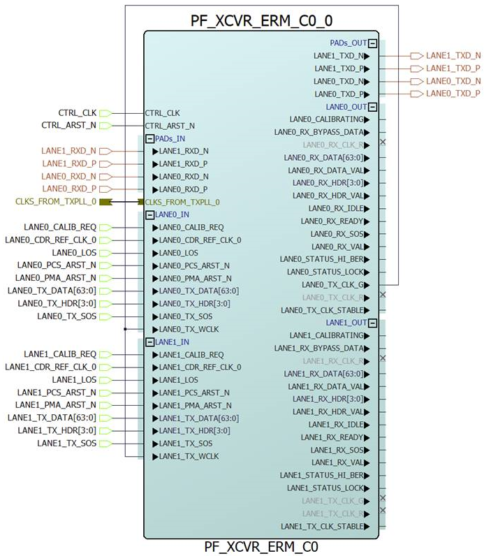
When Global-Shared mode is enabled, all the lanes include a global clock output port, but only one lane can be used as the master port. All the lanes include a TX_WCLK input port. This port must be connected to the global clock output of the master lane. The fly-wheel FIFO absorbs the phase difference between the lanes and the master lane’s global clock. See the following SmartDesign figure for an example.
- Regional: These clocks use local resources to interconnect with the FPGA fabric with a FIFO in the data path at the fabric boundary.
- Regional (Deterministic): These clocks use local resources to
interconnect with the FPGA fabric with zero-cycle data path at the fabric boundary
providing low-latency.
Microchip IP and solutions use these resources to optimize the FPGA architecture to provide robust use cases. See Table 1-16.