
1.3.2.6 64b67b Receive
(Ask a Question)Data comes into the 64b67b receiver from the PMA 32-bits per clock beat from the de-serializer. The data is qualified by RX_READY=1, which is set by the greater PMA logic when CDR achieves bit lock and is producing a stable clock.
The receive gearbox frames the 67-bit blocks by examining sync header bits [1:0] in the same method as described for 64b66b. The difference is in the span of bits between sync headers. The receive disparity block invert blocks as indicated by sync header bit [2]. The receive data is then sent to the fabric in 64-bit or 32-bit clock beat sequences. The 32-bit sequence is shown in the following figure where two clock beats transfer one symbol. In the 32-bit width, the sequence is 134 clock beats long and contains blank symbol transfers for clock beats 44-45, 88-89 and 132-133.
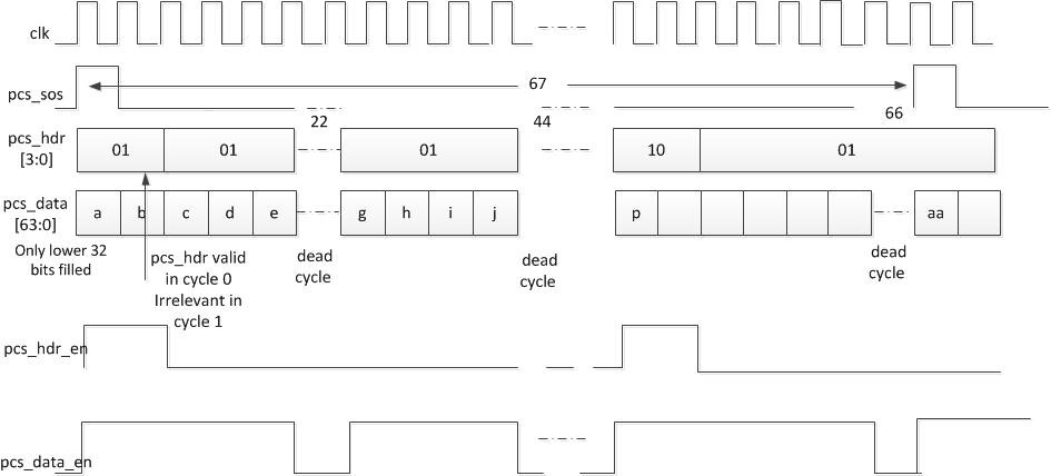
Sequence timing for the 64-bit interface consists of 67 clock beats with dead cycles at beats 22, 44, and 66.
The following table lists the port names and description for the 64b66b/64b67b mode of the PCS module. See section 49.2.4 of the IEEE® 802.3ae specification for more information.
| Port Name | Direction | Clock | Description |
|---|---|---|---|
| LANE#_CDR_REF_CLK_#/LANE#_CDR_REF_CLK_FAB | Input |
— | Reference clock to lane CDR. Can be sourced from either the FPGA clock or from a XCVR_#[A,B,C]REFCLK_P/N pin. |
| LANE#_REF_CLK | Input |
— | This port is exposed to user with
Half-Duplex option. LANE#_REF_CLK must be connected by the user to a
stable clock with same clock frequency as Recovered clock such as the
local clock. Note: LANE#_REF_CLK can be provided by
a separate PLL or CCC, however the LANE#_REF_CLK frequency must be
within ± 300 ppm with respect to LANE#_RX_CLK_R. |
| LANE#_TX_PLL_REF_CLK_# | Input |
— | Input clock from the TX_PLL REF_CLK_TO_LANE output pin. Included in CLKS_FROM_TXPLL_# BIF (bus interface). |
| LANE#_TX_BIT_CLK_0 | Input |
— | Clock from BIT_CLK of the XCVR TxPLL. Included in CLKS_FROM_TXPLL_# BIF (bus interface). |
| LANE#_TX_PLL_LOCK_# | Input |
— | Input lock status from the TX_PLL LOCK output pin. Included in CLKS_FROM_TXPLL_# BIF (bus interface). |
| LANE#_TX_SOS | Input | TX_CLK_[R:G] | Start-of-sequence pulse for a super frame, the length of which varies with the mode. |
| LANE#_TX_HDR[3:0] | Input | TX_CLK_[R:G] | Sync header corresponding to different encoding types. |
| LANE#_TX_DATA[63:0] | Input | TX_CLK_[R:G] | Input encoded data from fabric. PF_XCVR sends/receives bytes in high to low byte order only in the 64B6xB mode. |
| LANE#_PCS_ARST_N | Input | TX_CLK_[R:G] | Asynchronous active-low reset for PCS lane. |
| LANE#_PMA_ARST_N | Input | TX_CLK_[R:G] | Asynchronous active-low reset for the PMA lane. |
| LANE#_TX_ELEC_IDLE | Input | Asynchronous | Transceiver configurator allows pin to be exposed on component. This input forces XCVR_P/N transmit output pad pair to a common-mode voltage. It is used for low-frequency out-of-band signaling, or to signal entry into a low-power state to the link partner. |
| LANE#_TX_BYPASS_DATA | Input | Asynchronous | Transceiver configurator allows pin to be exposed on component. When LANE#_TX_BYPASS_DATA=1, the data can be driven into the transmit pads instead of the normal serializer data. The bypass is asynchronous and this signal does not transit through the FWF. This pin must be tied low if exposed to fabric and not used. |
| LANE#_RXD_N | Input |
— | Transceiver receiver differential input. |
| LANE#_RXD_P | Input |
— | Transceiver receiver differential input. |
| LANE#_RX_HDR_VAL | Output | RX_CLK_[R:G] | Enable for header data in |
| LANE#_RX_SOS | Output | RX_CLK_[R:G] | Start-of-sequence pulse for a super frame, the length of which varies based on the mode. High output indicates start of sequence. |
| LANE#_RX_DATA_VAL | Output | RX_CLK_[R:G] | Valid when there is data on RX_DATA. |
| LANE#_RX_HDR[3:0] | Output | RX_CLK_[R:G] | Sync header corresponding to different encoding types. |
| LANE#_RX_DATA[63:0] | Output | RX_CLK_[R:G] | Receive encoded data from 64b6b to the fabric. PF_XCVR sends/receives bytes in high to low byte order only in the 64B6xB mode. Bit 31 or bit 63 arrives first in the serial data. |
| LANE#_RX_VAL | Output | RX_CLK_[R:G] | LANE#_RX_VAL indicates that the XCVR
data path is initialized. The parallel bus of LANE#_RX_DATA[N:0]
contains actual data recovered from the serial stream when LANE#_RX_VAL
= 1. In 64b66b/64b67b mode, the Rx PCS logic self-resets when the CDR is not locked. In this mode, LANE#_RX_VAL rises just after LANE#_RX_READY rises. If you want to control Rx PCS reset, hold LANE#_PCS_ARST_N in reset when LANE#_RX_READY is low and release, when LANE#_RX_READY goes high. Once LANE#_PCS_ARST_N is released from reset, LANE#_RX_VAL rises to indicate the Rx parallel data is valid. In 64b6xb mode, the RX_VAL is qualified when the XCVR receiver calibration completes, included with the enhanced receiver management completion, and the CDR locks. |
| LANE#_RX_READY | Output |
— | Rises when the enhanced receiver
management and CDR completes a fine lock detection to the incoming data
transitions and the de-serializer is powered-up. If there is no incoming
data to the CDR then the RX_READY is low. The primary purpose of this
pin is communicating to fabric that the CDR is locked to serial input
data and is producing valid clocking. Note: In a loopback case while looping the local transmitter output to the receiver input, it is necessary to take the Tx out of reset to ensure valid serial transitions, allowing the Rx CDR to lock. The system deadlocks, if the user waits till Rx CDR locks before the Tx is released from reset. |
| LANE#_RX_IDLE | Output |
— | Receive electrical-idle detection flag. LANE#_Rx_IDLE peak detector logic is only valid for a limited minimum density of transitions on the Rx data and not to be used in applications above 5 Gbps. |
| LANE#_TX_CLK_STABLE | Output |
— | Transmit transceiver/PCS lane ready flag. |
| LANE#_RX_CLK_[R:G] | Output |
— | Global or regional receive clock to the fabric for the receiver. |
| LANE#_TX_CLK_[R:G]1 | Output |
— | Global or regional transmit clock to the fabric for the transmitter. |
| LANE#_STATUS_HI_BER | Output | RX_CLK_[R:G] | From the bit error rate monitor, which counts bad sync header values (0b00 or 0b11). Occurs over 125 µs interval. |
| LANE#_STATUS_LOCK | Output | RX_CLK_[R:G] | From the selected receive sync lock state-machine (Clause 49 or Clause 82). This is 0 when the sync header boundary is not locked, and it is 1 when sync lock is achieved. See IEEE 802.3 Clause 49 and Clause 82 for block lock state machine. |
| LANE#_TXD_N | Output |
— | Transceiver transmitter differential output. |
| LANE#_TXD_P | Output |
— | Transceiver transmitter differential output. |
- In PolarFire FPGA MPF500 devices, RT PolarFire RTPF500 devices, and PolarFire SoC FPGA Devices, the TX_CLK_R and RX_CLK_R pins of XCVR lanes placed in the PCIESS(Q0) and GPSS1(Q1) quads cannot drive I/Os.
- LANE# can be 0, 1, 2, and 3. [R:G] naming is generated based on the use of regional or global resources that are selected using Libero.