
2.9.4 Configuring the DDR4 Subsystem
(Ask a Question)The PF_DDR4 macro located in the Libero IP catalog must be instantiated in SmartDesign to access the DDR memory from the FPGA fabric. The following figure shows the DDR4 Configurator that configures the DDR4 subsystem. It supports the following modes:
- Preset configuration—allows selection from a list of memory vendors
and devices to preset all of the memory initialization and timing parameters
into the DDR Configurator, as shown in Figure 2-62.Important: For DDR4, preset configuration is supported for 1600, 1866, 2133, 2400, 2666, 2933, and 3200 at 800 MHz (minimum tCK ≥ 1.25 ns).
Figure 2-62. PF_DDR4 Configurator—Preset Configuration 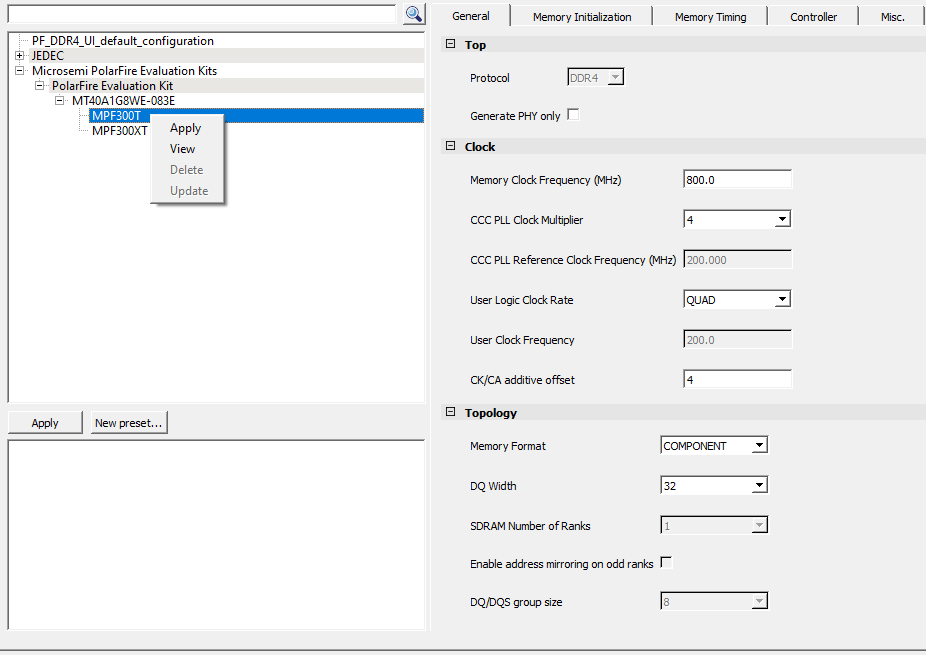
- User configuration—allows manual configuration of all memory initialization and timing parameters. This can be saved as a preset configuration, as shown in the preceding. See the DDR4 vendor datasheets before configuring DDR4 parameters.
General
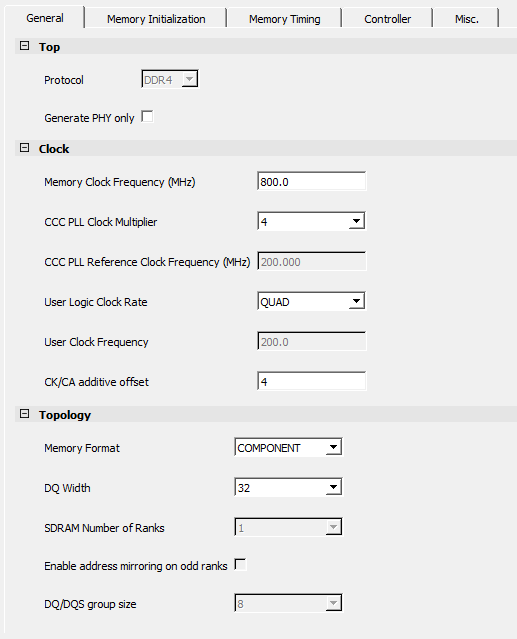
As shown in the preceding figure, the General tab provides the following options.
- Top
- Protocol: By default, this is set to DDR4.
- Generate PHY only: Enable this option to create a PHY-only DDR4 subsystem.
- Clock: To set
the DDR4 memory clock frequency and user logic clock rate. The user
clock frequency is automatically populated.
- Memory Clock Frequency (MHz): By default, the clock frequency is set to 800 MHz. The value must be within 0–800 MHz
- CCC PLL Clock Multiplier: Valid range is 1–49
- CCC PLL Reference Clock Frequency (MHz) : Depends upon Memory Clock Frequency (MHz) and CCC PLL Clock Multiplier. The value is 200 MHz when memory frequency is 800 MHz and clock multiplier is 4.
- User Logic Clock Rate: QUAD
- User Clock Frequency: Depends upon Memory Clock Frequency (MHz) and CCC PLL Clock Multiplier. The value is 200 MHz when memory frequency is 800 MHz and clock multiplier is 4.
- CK/CA additive offset: The value must be within 0–7. The default value is 4.
- Topology: To
set the topology of the memory system, including the address bits,
bank configurations, DM modes, and ECC.
- Memory Format: COMPONENT or type of DIMM (UDIMM, RDIMM, LRDIMM, or SODIMM)
- DQ
Width: 16-bit, 32-bit, or 64-bitImportant: AXI width must be larger than the data width and clock rate.
- SDRAM Number of Ranks: 1
- Enable Address mirroring on odd ranks: Disabled
- DQ/DQS group size: 8
- Row Address width: The value must be within [13, 17] range
- Column Address Width: 10
- Bank Address width: 2
- Bank Group Address width: The value must be within [1, 2] range
- Enable DM: OFF or DM (enabled)
- Enable Parity/Alert: When the memory format is RDIMM or LRDIMM, this option can be selected to support the Alert signal from DDR memory when it detects a CA parity error.
- Enable ECC: Check box toggle option
- Number of clock outputs: 1
Memory Initialization

As shown in the preceding figure, the Memory Initialization tab provides the following options.
- Mode
Register 0
- Burst length: Fixed BL8 or
On-the-fly BC4 or BL8Important: On-the-fly BC4 or BL8 option for burst length mode is not supported for QUAD clock rate.
- Read Burst Type: Sequential or Interleaved
- Memory CAS Latency: Value must be within 9–32
- Burst length: Fixed BL8 or
On-the-fly BC4 or BL8
- Mode
Register 1
- ODT Rtt Nominal Value: Any
one of the following options can be selected:
- Disabled
- RZQ/4
- RZQ/2
- RZQ/6
- RZQ/1
- RZQ/5
- RZQ/3
- RZQ/7
- Memory Additive CAS
Latency: Any one of the following
option can be selected:
- Disabled
- CL-1
- CL-2
- Output Drive Strength: RZQ/7 or RZQ/5
- ODT Rtt Nominal Value: Any
one of the following options can be selected:
- Mode
Register 2
- Low Power Auto Self Refresh
: Any one of the following options can
be selected:
- Manual - Normal
- Manual - Reduced
- Manual - Extended
- Automatic
- Memory Write CAS Latency:
Any one of the following options can be selected:
- 9
- 10
- 11
- 12
- 14
- 16
- 18
- 20
- Dynamic ODT (Rtt_WR): Any
one of the following option can be selected:
- Disabled
- RZQ/2
- RZQ/1
- High-Z
- RZQ/3
- Low Power Auto Self Refresh
: Any one of the following options can
be selected:
- Mode
Register 3
- Fine Granularity Refresh
Mode: Any one of the following options
can be selected:
- Normal mode (Fixed 1x)
- Fixed 2x
- Fixed 4x
- On-the-fly 1x/2x
- On-the-fly 1x/4x
- Fine Granularity Refresh
Mode: Any one of the following options
can be selected:
- Mode
Register 4
- Temperature Refresh Range: Normal or Extended
- Temperature Refresh Mode: Disabled or Enabled
- Internal VRef Monitor: Disabled or Enabled
- Self Refresh Abort Mode: Disabled or Enabled
- Read Preamble: 1CK or 2CK
- Write Preamble: 1CK
- Mode
Register 5
- CA Parity Latency Mode:
Any one of the following options can be selected:
- Disabled
- 4 clocks
- 5 clocks
- 6 clocks
- 8 clocks
- ODT Input Buffer for Power-down: Disabled or Enabled
- Park ODT Value(Rtt_Park):
Any one of the following options can be selected:
- Disabled
- RZQ/4
- RZQ/2
- RZQ/6
- RZQ/1
- RZQ/5
- RZQ/3
- RZQ/7
- CA Parity Latency Mode:
Any one of the following options can be selected:
- Mode
Register 6
- Vref Calibration Range: Range1 (60%–92.5%)
- Vref Calibration Value: 70.40
Memory Timing
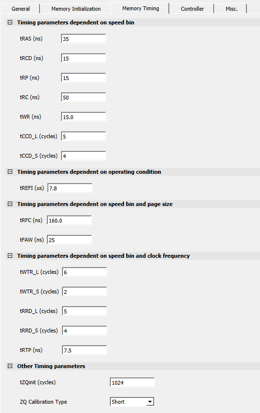
As shown in the preceding figure, the Memory Timing options provides the following options.
- Timing
parameters dependents on speed bin
- tRAS (ns): By default, preset configuration for the MT40A1G8WE-083E part is selected. Preset values for different configurations according to the JEDEC standard are supported. See the speed bin and its corresponding value in the vendor datasheet.
- tRCD (ns): By default, preset configuration for the MT40A1G8WE-083E part is selected. Preset values for different configurations according to the JEDEC standard are supported. See the speed bin and its corresponding value in the vendor datasheet.
- tRP (ns): By default, preset configuration for the MT40A1G8WE-083E part is selected. Preset values for different configurations according to the JEDEC standard are supported. See the speed bin and its corresponding value in the vendor datasheet.
- tRC (ns): By default, preset configuration for the MT40A1G8WE-083E part is selected. Preset values for different configurations according to the JEDEC standard are supported. See the speed bin and its corresponding value in the vendor datasheet.
- tWR (ns): By default, preset configuration for the MT40A1G8WE-083E part is selected. Preset values for different configurations according to the JEDEC standard are supported. See the speed bin and its corresponding value in the vendor datasheet.
- tCCD_L (cycles): By
default, preset configuration for the
MT40A1G8WE-083E part is selected. Preset values for
different configurations according to the JEDEC
standard are supported. See the speed bin and its
corresponding value in the vendor datasheet.Important: tCCD_L is equivalent to the data rate in the JEDEC specification. tCCD_L parameter field accepts a value in the range of 4–20, and the value entered gets routed to Mode Register 6 (MR6) bits[12:10].
- tCCD_S (cycles): By default, preset configuration for the MT40A1G8WE-083E part is selected. Preset values for different configurations according to the JEDEC standard are supported. See the speed bin and its corresponding value in the vendor datasheet.
- Timing
parameters dependents on operating
condition
- tREFI (us): By default, preset configuration for the MT40A1G8WE-083E part is selected. Preset values for different configurations according to the JEDEC standard are supported. See the speed bin and its corresponding value in the vendor datasheet.
- Timing
parameters dependents on speed bin and page
size
- tRFC (ns): By default, preset configuration for the MT40A1G8WE-083E part is selected. Preset values for different configurations according to the JEDEC standard are supported. See the speed bin and its corresponding value in the vendor datasheet.
- tFAW (ns): By default, preset configuration for the MT40A1G8WE-083E part is selected. Preset values for different configurations according to the JEDEC standard are supported. See the speed bin and its corresponding value in the vendor datasheet.
- Timing
parameters dependents on speed bin and clock
frequency
- tWTR_L (cycles): By default, preset configuration for the MT40A1G8WE-083E part is selected. Preset values for different configurations according to the JEDEC standard are supported. See the speed bin and its corresponding value in the vendor datasheet.
- tWTR_S (cycles): By default, preset configuration for the MT40A1G8WE-083E part is selected. Preset values for different configurations according to the JEDEC standard are supported. See the speed bin and its corresponding value in the vendor datasheet.
- tRRD_L (cycles): By default, preset configuration for the MT40A1G8WE-083E part is selected. Preset values for different configurations according to the JEDEC standard are supported. See the speed bin and its corresponding value in the vendor datasheet.
- tRRD_S (cycles): By default, preset configuration for the MT40A1G8WE-083E part is selected. Preset values for different configurations according to the JEDEC standard are supported. See the speed bin and its corresponding value in the vendor datasheet.
- tRTP (ns): By default, preset configuration for the MT40A1G8WE-083E part is selected. Preset values for different configurations according to the JEDEC standard are supported. See the speed bin and its corresponding value in the vendor datasheet.
- Others
Timing parameters
- tZQinit (cycles): By default, 1024 is selected. The value must be within [1024, 4095] range
- ZQ Calibration Type: Short or Long
- tZQCS (cycles): By default, 128 is selected. The value must be within [128, 2047]
- tZQoper (cycles): This value is fixed to 512.
- Enable User ZQ Calibration Controls: Enable or Disable. By default, this option is disabled.
- Automatic ZQ Calibration Period
(us): By default, 200 µs is selected.
For every 200 µs, ZQ calibration is triggered based
on the ZQCL or ZQCS cycles selected.Important:
- By default, preset configuration for the MT40A1G8WE-083E part is selected. Preset values for different configurations according to the JEDEC standard are supported. See the speed bin and its corresponding value in the vendor datasheet.
Controller

As shown in the preceding figure, the Controller tab provides the following options.
- Instance
Select: Enables the option to select the DDR4
subsystem instance number that is used to unify the controller
instance. PolarFire family supports a maximum of six DDR4 subsystem
instances.
- Instance Number:
-
User Interface
- Fabric Interface: options are AMBA AXI3/4 and native interface. The following table lists the supported AXI bus data widths with respect to the DQ widths.
- Data Bus Turnaround—provides additional bus turnaround time between different SDRAM ranks. The turnaround time is the number of clock cycles it takes to change the access from one rank to another rank for back-to-back memory accesses (read to read, read to write, write to write, and write to read). The AXI interface address is mapped based on the type of the Address Ordering selected in the PF_DDR4 configurator. For example, if Chip-Row-Bank-Col is selected, and if a row address width and column address width is configured for 13 and 11, the AXI address is mapped as shown in the following table.
Table 2-32. Supported AXI Bus Data Width DQ Width Supported AXI Data Bus Width x16 64, 128 x32 64, 128, 256 x64 512 -
Table 2-33. AXI Address Mapping AXI Address 31 30 29 28 27 26 25 24 23 22 21 20 19 18 17 16 15 14 13 12 11 10 9 8 7 6 5 4 3 2 1 0 Column Address C10 C9 C8 C7 C6 C5 C4 C3 C2 C1 C0 Bank Address BA2 BA1 BA0 Row Address R12 R11 R10 R9 R8 R7 R6 R5 R4 R3 R2 R1 R0 Important: The address mapping shown in the preceding table is applicable to Native interface also. - AXI Width: 64, 128, 256, or 512
- AXI ID Width: Valid range is 1–8
- Efficiency:
Provides control over memory refresh, precharge, and address ordering
options.
- Enable Activate/Precharge look-head: Check box toggle option
- Number of Banks to lookup: 4, 8, or 16
- Address Ordering: Any one of
the following options can be selected:
- Chip-Row-BG-Bank-Col
- Chip-BG-Bank-Row-Col
- Chip-Row-BG1-Bank-Col-BG0Important: Number of banks to lookup must be 8 or 16 when address ordering is set to Chip-Row-BG1-Bank-Col-BG0.
- ODT Activation Setting on
Write: provides options to enable ODT on write
operations.
- Enable Rank0 - ODT0: Enabled by default. Can Disabled or enabled.
- Enable Rank0 - ODT1: Not supported
- Enable Rank1 - ODT0: Not supported
- Enable Rank1 - ODT1: Enabled (fixed).
- Low Power
- Enable self request refresh control: When selected, this option saves power
- Misc
- Enable RE-INIT Controls: When selected, the configurator exposes the CTRLR_INIT signal. The initialization begins when this signal is asserted high for minimum 4 clock cycles in the fabric clock domain.
DDR4 Additional Controller Options
For DDR4, the Controller tab includes the following additional settings under Efficiency.
- The Address
Ordering includes the additional setting
Chip-Row-BG1-Bank-Col-BG0.
This selection will map the LSBs of an address to the BG0 field of the memory. This results in alternating Bank Groups during a burst operation based on the tCCD_S timing parameter (see memory device datasheet for tCCD_S settings). The tCCD_S parameter is the timing parameter which results in a better efficient operation for the DDR IP Configurator in the DDR4 mode.
Figure 2-67. Address Ordering—Chip-Row-BG1-Bank-Col-BG0 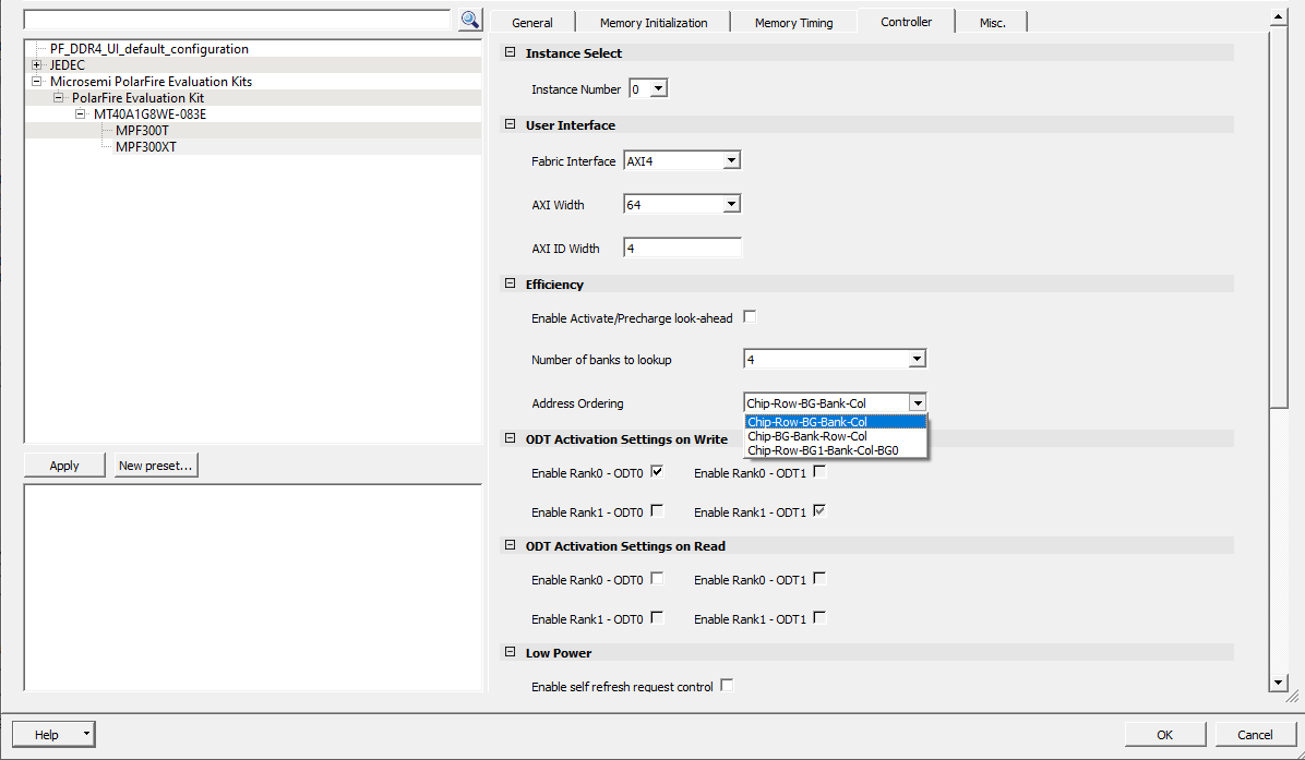
- The Number of banks to look up option includes
additional selections for 8 and 16. The default selection is 4.
This must be set to the number of banks in a Bank Group of the DDR4 memory device being used. Selecting a higher value is more challenging in terms if timing closure on the controller. A setting of 8 works for all but the most congested designs. A setting of 16 works for designs that have 15% timing margin or more.
Figure 2-68. Number of Banks to Look Up 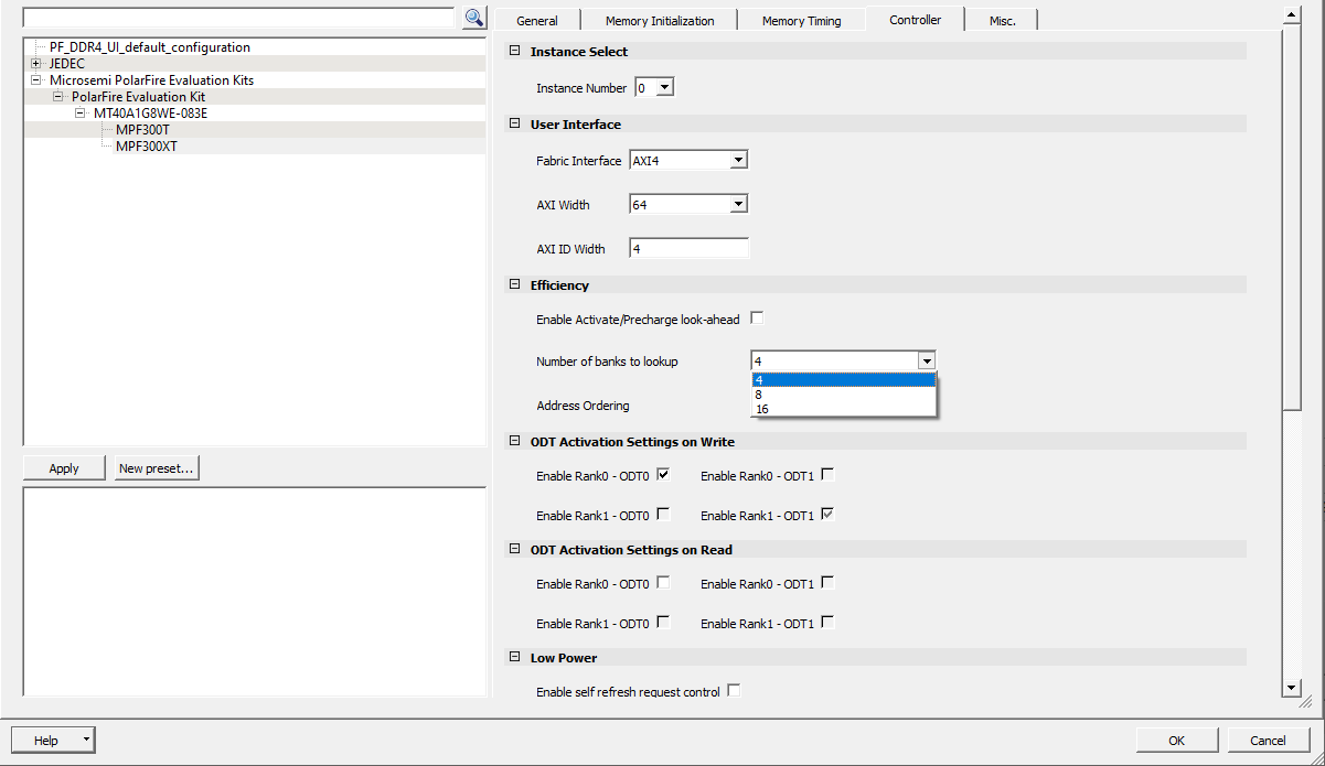
Miscellaneous

As shown in the preceding figure, the Misc. options provides the following options.
- Simulation
Options
- Simulation
mode:
- Fast (skip training and settling time): In this mode, the DDR4 subsystem skips the DDR4 training sequence and asserts CTRLR_READY without waiting for the settling time. CTRLR_READY is asserted within 8 μs.
- Training (skip settling time): In this mode, the DDR4 subsystem performs the DDR4 training sequence but asserts CTRLR_READY without waiting for settling time. CTRLR_READY is asserted within 240 μs.
- Full (training and settling time): In this mode, the DDR4 subsystem performs the DDR4 training sequence and also waits for settling time before asserting CTRLR_READY. In this mode, CTRLR_READY is asserted within 10 ms.
- Simulation
mode:
- Throughput
Options
- Pipe Lining: Adds pipeline registers to Training IP (TIP) write and read data path to improve static timing closure.