
1.3.10 Configuring Current, Differential Voltage, Temperature, and Voltage Peripherals
The Current, Differential Voltage, Temperature, and Voltage peripherals are all configured the same way. Also, the effects of averaging are the same for all peripherals in the Analog System Builder.
Minor variations, such as Maximum Voltage in the Voltage monitor, are explained in the help topic for that peripheral. Signal name is the name of the signal as you want it to appear in the main Analog System Builder dialog box.
Digital filtering
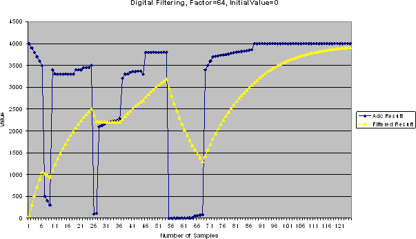
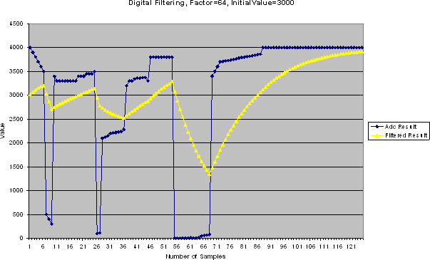
Once the ADC finishes converting the analog signal to a digital value, it filters (averages) the resulting digital output. Digital filtering is a single-pole low-pass filter built in soft gates; you can use it to improve the signal-to-noise ratio. If the ADC input data is very erratic, the filtering will smooth out the input and reduce the noise.
The filtered value is calculated using the following equation:
If the Digital filtering factor is set to 1, it is ignored.
In some cases, where the inputs are very low frequency, and the electrical environment is not very noisy, it may be possible to proceed without any special filtering of input analog signals. However, in most applications it is desirable to at least implement a simple post-conversion digital filter inside the FPGA by oversampling and averaging several results to reduce the effects of random noise in the conversion signal path and improve overall accuracy. This simple averaging is automatically handled in the software by setting the Digital Filtering factor in the Analog System Builder (ASB) to specify how many samples are averaged (when the factor is N, 2**N samples are averaged together).
For situations where greater accuracy is required, an external analog filter may be needed to eliminate non-random and out-of-band noise sources. If an analog filter is not used to restrict the input signal content to the band-of-interest, any out-of-band signals or noise will be aliased into the conversion result as random in-band noise.
Some applications (for example, those that require frequency detection) may need both external analog filtering to limit out-of-band effects, and more sophisticated digital processing such as a multi-tap Finite Impulse Response (FIR) filter. A wide variety of digital filtering methods are available through the FPGA gates available in a Fusion Device.
Initial Filtering Value - The initial filtering value enables you to specify the starting value for the averaging function (Filtering Result[0]). This enables you to ‘seed’ your filtering function so that there are no erroneous values produced during the beginning of operation. If you do not use an initial filtering value, the filtering function always starts with FilteringResult[0] = 0, thereby skewing the results towards 0 during the first range of samples.
Range - The Initial value range for the digital filter is identical to the threshold range for the peripheral.
The system instantiates the logic required to perform averaging as soon as there is at least one channel in the system that requires averaging. There is no extra logic penalty for averaging the other channels of the system. See the figures below for a graphical representation of the effect of digital filtering on a signal.
Acquisition Time
The required settling/sampling time for this channel. It is the amount of time the Sample and Hold circuit in the ADC charges the capacitor with the input analog signal. The characteristics of your system and monitoring requirements will determine this value. Note also that this value has a direct correlation to the achievable sampling rate of the system.
The prescaler logic of the AB has a settling time of 10s max. It is an application-dependent setting and must be accounted for by you via the acquisition and hold time for each channel. A recommended default value is inserted by ASB when configuring a new Voltage Monitor but it may be reduced, with a possible reduction in sampling accuracy.
ASB evaluates the required acquisition times for all peripherals and the system frequency to compute the maximum possible ADC clock frequency. Only certain divider factors exist to create the ADC Clock; because of this and peripheral acquisition times, certain system frequencies result in a faster ADC Clock.
Signal Polarity - Current and Differential Voltage Peripherals ONLY
Use this option to change polarity. The associated voltage monitor must be configured with the same polarity. During simulation, a negatively configured peripheral must be driven by negative voltage values.
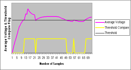
Comparison Flag Specification - Once the software calculates the average, you can further process the result by comparing the result to a given threshold and deciding under what conditions to assert the comparison flags.
Select a flag and click the Delete button to delete it.
Click the Add Flag button to add more flags to the system.
Flag Name - This is the name of the flag. This will appear as the output port name in the final output. It will be prefixed with the signal name with which it is associated, to group the input and outputs together.
Flag Type - You can choose to assert the flag when the signal is either under a given threshold or over a given threshold.
Threshold - Threshold value. The following figure shows the effect of the threshold on a given signal.
Assert Samples - The number of consecutive samples on this channel that reach or exceed the threshold for the flag to assert. This can be a glitch removal feature. If it is set to 1, the final flag is identical to the comparison result.
For example, if your Assert Sample value is 5 and the threshold is set at 3.0V, the channel must reach or exceed 3.0V five times in a row on this channel for the flag to assert. If your voltage values are less than 3.0V, the flag will not assert. The figure below shows the effect of glitch removal on a given signal.
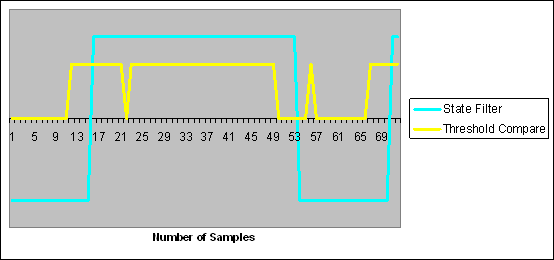
De-assert Samples - The number of consecutive samples of this channel that are not above the threshold required for the flag to de-assert once it has been asserted. This is a glitch removal feature. If this value is set to 1, the final flag is identical to the comparison result.
For example, if your de-assert Sample value is 10 and the threshold is set at 3.3V, you must have 10 consecutive samples that go below 3.3V in order for the flag to de-assert