
6.5 I/O Attributes Editor
6.5.1 Using I/O Attribute Editor with SmartDesign
You can use the I/O Attribute Editor to assign I/Os in SmartDesign, and SmartDesign will automatically generate the PDC file and pass it to Designer.
When you open an existing PDC file that was generated by SmartDesign, the SmartDesign associated with that PDC file automatically opens.
6.5.2 Enabling the I/O Attribute Editor in SmartDesign
To enable the I/O Attribute Editor in SmartDesign:
- From the SmartDesign menu, choose
Show I/O Attribute Editor View. The I/O Attribute Editor opens in front of the
SmartDesign Canvas (as shown below).
Figure 6-15. I/O Attribute Editor in SmartDesign 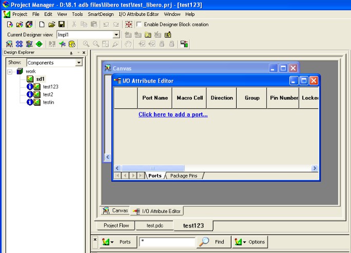
- Click the Canvas tab, and then select the component to modify.
- Click the I/O Attribute Editor tab to modify the I/O attributes of the selected component.
6.5.3 Using the I/O Attribute Editor with the Canvas
Using the I/O Attribute Editor with the Canvas
When you open a file in SmartDesign, the port list is populated.
If a port is added, modified, or deleted from the SmartDesign Canvas or Grid, it is automatically updated in the I/O Attribute Editor.
The I/O constraints are automatically passed from SmartDesign to Designer through a PDC file.
6.5.4 I/O Attribute Editor Menu
This menu is available from the I/O Attribute Editor in Libero IDE.
|
Command |
Icon |
Shortcut |
Function |
|---|---|---|---|
|
Add Port |
Displays the Add New Port dialog box, in which you can add a new port to the design | ||
|
Modify Port |
Displays the Modify Port dialog box, in which you can change the name and direction of the port | ||
|
Delete |
Deletes the selected port | ||
|
Unassign from Location |
CTRL + SHIFT + K |
Unassigns the selected port from its current location | |
|
Unassign All from Location |
Unassigns all ports from their locations | ||
|
Lock |
|
CTRL + L |
Locks the selected port |
|
Unlock |
|
CTRL + SHIFT + L |
Unlocks the selected locked port |
|
Lock All |
Locks all I/Os in your design | ||
|
Unlock All |
Unlocks all I/Os in your design | ||
|
Import I/O Assignments |
Displays the Open dialog box, in which you select the file to import |
6.5.4.1 I/O Attribute Editor > Tools
Command | Icon | Shortcut | Function |
|---|---|---|---|
I/O Bank Settings | CTRL + I | Displays the I/O Bank Settings dialog box, in which you can assign technologies and VREF pins to your I/O banks | |
|
Auto-Assign I/O Banks |
|
Assigns a voltage to every I/O bank that does not have a voltage assigned to it and if required, a VREF pin | |
|
Reserve Pins for Device Migration |
CTRL + M |
Displays the Reserve Pins for Migration dialog box. This dialog box enables you to automatically reserve pins that are not bonded in the destination device that you select. | |
|
Manage Groups |
Creates and manages the groups in the I/O Attribute Editor. You can also use this command to assign ports to a group. | ||
|
Remove All Constraints |
Removes all constraints from all ports. You can use the Undo command to put them back. |
6.5.4.2 I/O Attribute Editor > Format
Command | Icon | Shortcut | Function |
|---|---|---|---|
Row > Hide | Hide the selected row(s) | ||
Row > Unhide | Show all hidden rows between the selected rows | ||
Column > Hide | Hide the selected column(s) | ||
Column > Unhide | Show all hidden columns between the selected columns | ||
Column > Freeze Pane | Freeze the selected columns(s) | ||
Column > Unfreeze Pane | Unfreeze all columns(s) | ||
Column > Autofit | Sets the width of columns within the table to accommodate all the text for any given row in those columns, including the column headings |
6.5.5 Add New Port Dialog box
To access this dialog box, from the I/O Attribute Editor menu, choose Add Port. You can also right-click a row in the
- Name
- Enter a name for the new port.
- Direction
- Select one of the following options:
- Input
- Select this option if the port is to receive a signal.
- Output
- Select this option if the port is to send a signal.
- Bi-directional (Inout)
- Select this option if the port will both send and receive a signal.
6.5.6 Modify Port Dialog box
To access this dialog box, from the I/O Attribute Editor menu, choose Modify Port. You can also right-click a row in the Ports tab of the I/O Attribute Editor, and choose Modify Port to display this dialog box.
- Name
- Enter a new name for the port.
- Direction
- Select one of the following options:
- Input
- Select this option if the port is to receive a signal.
- Output
- Select this option if the port is to send a signal.
- Bi-directional (Inout)
- Select this option if the port will both send and receive a signal.
6.5.7 I/O Bank Settings Dialog Box (IGLOO and ProASIC3 only)
To access this dialog, from the Edit menu, choose I/O Bank Settings.
Use this dialog box to assign I/O technologies to I/O banks in IGLOO (excluding IGLOOe) and ProASIC3 (excluding ProASIC3L and ProASIC3E) devices.
6.5.7.1 Choose Bank
Choose a bank from the drop-down list. If you do not assign I/O standards to a bank, that bank uses the default standard selected in the Device Selection Wizard.
6.5.7.2 Locked
Select this option to lock all I/O banks, so the I/O Bank Assigner cannot unassign and re-assign the technologies in your design.
6.5.7.3 Select All Technologies That the Bank Should Support
Selecting an I/O standard selects all compatible standards and grays out incompatible ones. For example, selecting LVTTL also selects PCI, PCIX, and LVPECL, since they all have the same VCCI. Further, selecting GTLP (3.3V) disables SSTL3 as an option because the VREFs of the two are not the same.
6.5.7.4 VCCI
Each I/O bank has a common supply voltage, VCCI, for the I/Os within that bank.
Click Apply to assign the selected I/O standards to the selected bank. Any previously assigned I/Os in the bank that are no longer compatible with the standards applied are unassigned.
6.5.8 I/O Bank Settings Dialog Box
To access this dialog, from the Edit menu, choose I/O Bank Settings.
Use this dialog box to assign I/O technologies to I/O banks in IGLOOe, Fusion, ProASIC3L, ProASIC3E, and Axcelerator devices.
6.5.8.1 Choose Bank
Choose a bank from the drop-down list. If you do not assign I/O standards to a bank, that bank uses the default standard selected in the Device Selection Wizard.
6.5.8.2 Locked
Select this option to lock all I/O banks, so the I/O Bank Assigner cannot unassign and re-assign the technologies in your design.
6.5.8.3 Select All Technologies That the Bank Should Support
Selecting an I/O standard selects all compatible standards and grays out incompatible ones. For example, selecting LVTTL also selects PCI, PCIX, and LVPECL, since they all have the same VCCI. Further, selecting GTLP (3.3V) disables SSTL3 as an option because the VREFs of the two are not the same.
6.5.8.4 VCCI
Each I/O bank has a common supply voltage, VCCI, for the I/Os within that bank. (Technologies not allowed for the selected VCCI appear grayed out.)
6.5.8.5 VREF
A voltage referenced I/O input (VREF) requires an input referenced voltage. You must assign VREF pins to IGLOOe, Fusion, ProASIC3L (A3PE3000L only), ProASIC3E, and Axcelerator devices before running Layout.
You cannot assign VREF pins in IGLOO or ProASIC3 low-cost devices.
6.5.8.6 Use Default Pins for VREFs
Select this check box to set default VREF pins and unset non-default VREF pins. If you unselect this option when setting a new VREF technology, no VREF pins are set. If you unselect this option when default VREF pins are already set, it unsets them.
Click More Attributesto set the low-power mode and input delay. (These attributes are not supported in IGLOOe, Fusion, ProASIC3E, or RTAXS devices.)
Click Apply to assign the selected I/O standards to the selected bank. Any previously assigned I/Os in the bank that are no longer compatible with the standards applied are unassigned.
6.5.9 I/O Bank Settings for the SmartDesign Microcontroller Subsystem (MSS)
To access the I/O Bank settings in your MSS design you must click the I/O Editor tab in the MSS configurator, and from the I/O Editor Menu choose I/O Bank Settings.
You can use the I/O Bank Settings dialog box to change the VCCI of the banks where the MSS I/Os are placed. Note: Note: These settings cannot be changed in Designer software.
You have four options:
- 1.50V
- 1.80V
- 2.50V
- 3.30V
East MSS I/Os refer to Bank2. West MSS I/Os refer to Bank4.
When changing the VCCI the MSS I/Os placed on this bank will change the IoTech to match the new VCCI; this is done automatically.
The IoTech is changed as follows:
- 3.30V: MSS I/Os placed on this bank are changed to LVTTL.
- 2.50V: MSS I/Os placed on this bank are changed to LVCMOS 2.5V.
- 1.80V: MSS I/Os placed on this bank are changed to LVCMOS 1.8V.
- 1.50V: MSS I/Os placed on this bank are changed to LVCMOS 1.5V.
6.5.10 More I/O Bank Attributes Dialog Box
To access this dialog, from the Edit menu, choose I/O Bank Settings, and then click More Attributes.
Use this dialog box to configure these low-power mode settings:
- Enable/disable input/output buffers
- Input delay for a bank
Although designed for high performance, the Axcelerator architecture also allows you to place the device into a low-power (LP) mode via a dedicated LP pin. Asserting the LP pin, which is grounded in normal operation, activates LP mode on all the I/O banks. When LP mode is activated, I/O banks are disabled (inputs disabled, outputs tristated), and PLLs are placed in a power-down mode. All internal register states are maintained in this mode. Furthermore, you can configure individual I/O banks to opt out of the LP mode, giving you access to critical signals while the rest of the chip is in LP mode.
Using the following options in the More Attributes dialog box, you can individually configure each I/O bank in an Axcelerator device when in low-power mode:
6.5.10.1 Low-Power Mode
- Enable Input Buffers- Select to enable input buffers. If this option is selected, all used input buffers within this bank will remain enabled whether or not the LP pin is asserted.
- Enable Output Buffers - Select to enable output buffers. If this option is selected, all used output buffers within this bank will remain enabled whether or not the LP pin is asserted.
6.5.10.2 Input Delay
Drag the slider bar to your desired delay. The delay is bank-specific. The delay code and typical value appear. Click View All Delays to see all the delay values (Best, Worst, Typical, Rise-Rise, Fall-Fall) for the input delay selected. You must select a technology to see the input delays.
The Low-Power mode option is not supported in the IGLOO (all devices), ProASIC3 nano, ProASIC3L, Fusion and RTAX-S families.
For more information, refer to the datasheet for your device. Datasheets are available from the Microchip website.