
10.2.6 Axcelerator® PLL
The Axcelerator® PLL is a clock management core that provides clock delay minimization, clock frequency synthesis and programmable clock adjustment capabilities.
Related Topics
Key Features
- Clock Delay Minimization
- Clock Frequency Synthesis
- Programmable delay lines for clock delay adjustment
- 6-bit divider in the feedback path for clock multiplication
- 6-bit divider in one of the output paths for clock division
- Cascadable up to two PLLs
The Axcelerator PLL has three main features. They are:
Clock Delay Minimization
In this mode the PLL can perform either a positive or negative clock delay operation of up to 3.75 ns in increments of 250 ps before or after the clock edge of the incoming reference clock. The value of the delay is programmable through the five bits of the DelayLine bus.
Clock Frequency Synthesis
The multiplier and divider can be used together to synthesize a wide range of output frequencies from the reference clock. Input frequencies are allowed to be in the range of 14 MHz to 200 MHz. Multiplication and division factors are integers in the range of 1 to 64. The maximum allowable output frequency is 1 GHz. The output duty cycle is fixed at 50/50.
Cascading Blocks
The device supports cascading of up to 2 PLLs.
The Axcelerator family provides eight PLLs, four on the north side and four on the south side of the device. The outputs of the north-side PLLs can be connected to either hard-wired clock networks or regular nets. The outputs of the south-side PLLs can be connected to either routed clock networks or regular nets. The Axcelerator family PLLs have many outstanding features, including the following:
- PLLs can multiply and/or divide the reference clock frequency by factors ranging from 1 to 64. As a result, there are many available output frequencies for each PLL, based on the input frequency. The software automatically calculates the values of the multiplier and divider based on the Input and Output frequencies specified. If the exact value cannot be achieved, the core configurator generates the output frequency that is the closest possible to the required value.
- PLLs are capable of inserting programmable delays on the REF Clock from –3.75 ns to +3.75 ns with the steps of 250 ps. The delay is programmed either statically or dynamically. Dynamic programming means that you can change the delay value during the operation when the device is functional. If you select the dynamic delay, then the 5-bit Delay Line port is added to the generated code and accessible to you.
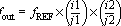
Refclk is the reference input to the PLL. The frequency of Refclk can vary from 14 MHz to 200 MHz. The reference can be supplied from a dedicated pad or an internal net.
You can select to have an internal or external feedback. Selecting an external feedback adds a port (named FB) to the PLL block, through which the external feedback is passed into the PLL and the internal feedback is blocked.
Clk(freq) are the output signals from the PLL. The CLK(primary) is defined as refclk * i/j where i is the multiplier and j is the divider. CLK(secondary) is defined as refclk * i.
- Cascading
Cascading is an option that helps you generate a wider range of output frequencies. If cascading is set to No and the output frequency is chosen as a value that cannot be achieved by fREF * i/j, then the PLL tries to set i and j in order to reach to the closest vicinity of the desired frequency. If cascading is set to Y es, then for the conditions in which the desired frequency is unattainable by a single PLL, another PLL is cascaded to the first PLL and then the final output frequency is:
In cascading PLLs, the input frequency of each PLL should remain in the range of 14 MHz to 200 MHz.
You must specify the desired output frequencies and the networks that the outputs should drive for the PLL outputs CLK1 and CLK2.Note: If cascading is disabled, the CLK2 frequency can only be a multiple of the referencefrequency. As mentioned earlier, if the selected values for output frequencies cannot be achieved, they are set to the closest possible frequency.
For each output, there are three routing resources. Hard-wired is the HCLK network which reaches to the clock input of R-cells. Selecting a hard-wired output for the PLL implies that the PLL should be located at the north side of the device. If one of the outputs is connected to hard-wired global network, the routed clock network cannot be chosen as the second output because the routed clock network is only accessible by the PLLs on the south side. The software helps you select the output type by keeping the possible outputs active and disabling the illegal combinations.
Figure 10-48. Basic Axcelerator PLL Architecture 
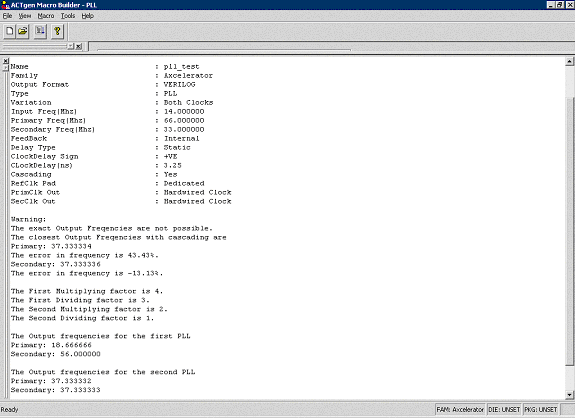
Message Log
All the parameters specified by the user and the values calculated by the core configurator software are saved in the <design>.log file (as follows).
For more detailed information on the various features of the Axcelerator PLL, please refer to the Axcelerator Family PLL and Clock Management application note at www.Microchip.com