12.4.1 Clock/PLL Generators
The dsPIC33AK512MPS512 family of devices contain multiple clock generators (CLKGEN). The Clock/PLL generators can be configured for any clock source available. Clock generator 1 will act as the system clock, and it will always be enabled.
An expanded view of the CLKGEN is detailed in Figure 12-3.
The assignment of CLKGEN to peripherals is listed in Table 12-2.
The other clock generators can be configured for any clock source. For example, to reference FRC, set the COSC[3:0] bits to the FRC source and enable clock switching.
Each generator can be enabled either via setting the ON bit in the CLKxCON register or when requested by a consumer (e.g. a peripheral).
The ON bit is logically ORed with clock request signals from other peripherals to enable the CLKGEN or PLL, and it can only be used to disable the CLKGEN or PLL when there are no active clock requests. In addition, clearing the OSCCTRL.PLLxEN bit disables PLLx.
Each clock generator has a dedicated divider (CLKxDIV) and control bits.
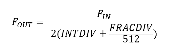
The INTDIV bitfield within CLKxDIV is an integer divider. It divides the clock frequency by the two multiplied by the value of INTDIV. The FRACDIV is a fractional divider that allows for intermediate dividing that is not possible by using the integer divider alone. The value of FRACDIV is divided by 512 to create a fraction that is added to the INTDIV value.
Equation 12-1 provides the relationship between the Clock Generator input frequency (FIN) and the Clock Generator output frequency (FOUT).
Equation 12-2 provides the relationship between the Clock Generator input frequency (FIN) and the Clock Generator FRACDIV value.