
43.32 Bluetooth® Low Energy RF Characteristics
| AC Characteristics | Standard Operating Conditions: VDDIO = VDDANA 1.9-3.6V (unless otherwise stated) Operating Temperature: -40°C ≤ TA ≤ +85°C for Industrial Temp -40°C ≤ TA ≤ +125°C for Extended Temp | ||||||
|---|---|---|---|---|---|---|---|
| Param. No. | Symbol | Characteristics | Min. | Typ. | Max. | Units | Conditions |
| BTG1 | FREQ | Frequency range of operation | 2402 | — | 2480 | MHz | — |
| BTTX1 | TXPWR:MPA | Bluetooth® transmit power MPA | — | 11.67 | — | dBm | — |
| BTTX2 | TXPWR:LPA | Bluetooth transmit power LPA | — | 3.95 | — | dBm | — |
| BTX3 | TXIB:1MBPS | In-band emission for FTX ± -2 MHz | — | -32 | — | dBm | — |
| In-band emission for FTX ± -(3+N) MHz | — | -45 | — | dBm | — | ||
| BTX4 | TXIB:2MBPS | In-band emission for FTX ± -4 MHz | — | -43 | — | dBm | — |
| In-band emission for FTX ± -5 MHz | — | -48 | — | dBm | — | ||
| In-band emission for FTX ± -(6+N) MHz | — | -51 | — | dBm | — | ||
| BTRX1 | RXSENSE | Receiver sensitivity at 1 Mbps | — | -97 | — | dBm | — |
| Receiver sensitivity at 2 Mbps | — | -94 | — | dBm | — | ||
| Receiver sensitivity at S = 8 | — | -104 | — | dBm | — | ||
| Receiver sensitivity at S = 2 | — | -101 | — | dBm | — | ||
| BTRX2 | MAXINSIG | Maximum input signal level at 1 Mbps | — | 0 | — | dBm | — |
| Maximum input signal level at 2 Mbps | — | 0 | — | dBm | |||
| Maximum input signal level at S = 2 | — | 0 | — | dBm | |||
| Maximum input signal level at S = 8 | — | 0 | — | dBm | |||
| BTRX3(3) | CI1M:COCH | C/I Co channel rejection | — | 8 | — | dB | — |
| CI1M: ± -1MHz | C/I adjacent channel rejection | — | 1 | — | dB | — | |
| CI1M: ± -2MHz | C/I adjacent channel rejection | — | -30 | — | dB | — | |
| CI1M:ADJ(3+n) | C/I alternate channel rejection | — | -48 | — | dB | — | |
| CI1M:IMG | C/I image frequency rejection | — | -24 | — | dB | — | |
| CI1M:IMG ± -1 MHz | C/I adjacent channel to image freq rejection | — | -31 | — | dB | — | |
| BTRX4(3) | CIS2:COCH | C/I Co channel rejection | — | 6 | — | dB | — |
| CIS2: ± -1MHz | C/I adjacent channel rejection | — | -6 | — | dB | — | |
| CIS2: ± -2MHz | C/I adjacent channel rejection | — | -38 | — | dB | — | |
| CIS2:ADJ(3+n) | C/I alternate channel rejection | — | -50 | — | dB | — | |
| CIS2:IMG | C/I image frequency rejection | — | -27 | — | dB | — | |
| CIS2:IMG ± -1 MHz | C/I adjacent channel to image freq rejection | — | -37 | — | dB | — | |
| BTRX5(3) | CIS8:COCH | C/I Co channel rejection | — | 7 | — | dB | — |
| CIS8: ± -1 MHz | C/I adjacent channel rejection | — | -7 | — | dB | — | |
| CIS8: ± -2 MHz | C/I adjacent channel rejection | — | -38 | — | dB | — | |
| CIS8:ADJ(3+n) | C/I alternate channel rejection | — | -48 | — | dB | — | |
| CIS8:IMG | C/I image frequency rejection | — | -27 | — | dB | — | |
| CIS2:IMG ± -1MHz | C/I adjacent channel to image freq rejection | — | -41 | — | dB | — | |
| BTRX6(3) | CI2M:COCH | C/I Co channel rejection | — | 8 | — | dB | — |
| CI2M: ± -2MHz | C/I adjacent channel rejection | — | 1 | — | dB | — | |
| CI2M: ± -4MHz | C/I adjacent channel rejection | — | -29 | — | dB | — | |
| CI2M:ADJ(6+2n) | C/I alternate channel rejection | — | -42 | — | dB | — | |
| CI2M:IMG | C/I image frequency rejection | — | -23 | — | dB | — | |
| CI2M:IMG ± -2MHz | C/I adjacent channel to image freq rejection | — | -28 | — | dB | — | |
| BTRX7(3) | BLOCK1M:<2GHZ | Blocking performance from 30-2 GHz | — | -10 | — | dBm | — |
| BLOCK1M:2 GHZ<SIG<2399MHz | Blocking performance from 2003-2399 MHz | — | -21 | — | dBm | — | |
| BLOCK1M:2484 MHZ<SIG<2977MHz | Blocking performance between 2484-2997 MHz | — | -15 | — | dBm | — | |
| BLOCK1M:3 GHZ<SIG<12.75GHz | Blocking performance between 3-12.5 GHz | — | -10 | — | dBm | — | |
| BTRX8(3) | BLE1M:INTERMOD | Inter modulation performance for BLEM | — | -36 | — | dBm | — |
| BLE2M:INTERMOD | Inter modulation performance for BLEM | — | -28.5 | — | dBm | — | |
Note:
| |||||||
| AC Characteristics | Standard Operating Conditions: VDDIO = VDDANA 1.9-3.6V (unless otherwise stated) Operating Temperature: -40°C ≤ TA ≤ +85°C for Industrial Temp | ||||||
|---|---|---|---|---|---|---|---|
| Param. No. | Symbol | Characteristics | Min. | Typ. | Max. | Units | Conditions |
| BTG1 | FREQ | Frequency range of operation | 2402 | — | 2480 | MHz | — |
| BTX1 | TXPWR:WBZ451H | Bluetooth® transmit power at 3.3V | — | 19.8 | — | dBm | — |
| Bluetooth transmit power at 2.5V | — | 18.6 | — | dBm | — | ||
| Bluetooth transmit power at 1.9V | — | 16.8 | — | dBm | — | ||
| BTX2 | TXIB:1MBPS | In-band emission for FTX ± 2 MHz | — | -26.2 | — | dBm | — |
| In-band emission for FTX ± (3+N) MHz | — | -37.8 | — | dBm | — | ||
| BTX3 | TXIB:2MBPS | In-band emission for FTX ± 4MHz | — | -34.6 | — | dBm | — |
| In-band emission for FTX ± 5 MHz | — | -40.1 | — | dBm | — | ||
| In-band emission for FTX ± (6+N) MHz | — | -43.3 | — | dBm | — | ||
| BTRX1 | RXSENSE | Receiver sensitivity at 1 Mbps | — | -99.6 | — | dBm | — |
| Receiver sensitivity at 2 Mbps | — | -96.6 | — | dBm | — | ||
| Receiver sensitivity at S = 8 | — | -107.1 | — | dBm | — | ||
| Receiver sensitivity at S = 2 | — | -103.6 | — | dBm | — | ||
| BTRX2 | MAXINSIG | Maximum input signal level at 1 Mbps | — | -10 | — | dBm | — |
| Maximum input signal level at 2 Mbps | — | -10 | — | dBm | — | ||
| Maximum input signal level at S = 2 | — | -10 | — | dBm | — | ||
| Maximum input signal level at S = 8 | — | -10 | — | dBm | — | ||
| BTRX3 | CI1M:COCH | C/I Co channel rejection | — | 14 | — | dB | — |
| CI1M:± 1MHz | C/I adjacent channel rejection | — | 14 | — | dB | — | |
| CI1M:± 2MHz | C/I adjacent channel rejection | — | 12 | — | dB | — | |
| CI1M:ADJ(3+n) | C/I alternate channel rejection | — | 9 | — | dB | — | |
| CI1M:IMG | C/I image frequency rejection | — | 13 | — | dB | — | |
| CI1M:IMG± 1MHz | C/I adjacent channel to image frequency rejection | — | 12 | — | dB | — | |
| BTRX4 | CIS2:COCH | C/I Co channel rejection | — | 12 | — | dB | — |
| CIS2:± 1MHz | C/I adjacent channel rejection | — | 19 | — | dB | — | |
| CIS2:± 2MHz | C/I adjacent channel rejection | — | 15 | — | dB | — | |
| CIS2:ADJ(3+n) | C/I alternate channel rejection | — | 15 | — | dB | — | |
| CIS2:IMG | C/I image frequency rejection | — | 11 | — | dB | — | |
| CIS2:IMG± 1MHz | C/I adjacent channel to image frequency rejection | — | 16 | — | dB | — | |
| BTRX5 | CIS8:COCH | C/I Co channel rejection | — | 8 | — | dB | — |
| CIS8:± 1MHz | C/I adjacent channel rejection | — | 15 | — | dB | — | |
| CIS8:± 2MHz | C/I adjacent channel rejection | — | 11 | — | dB | — | |
| CIS8:ADJ(3+n) | C/I alternate channel rejection | — | 14 | — | dB | — | |
| CIS8:IMG | C/I image frequency rejection | — | 7 | — | dB | — | |
| CIS2:IMG± 1MHz | C/I Adjacent channel to image frequency rejection | — | 14 | — | dB | — | |
| BTRX6 | CI2M:COCH | C/I Co channel rejection | — | 15 | — | dB | — |
| CI2M:± 2MHz | C/I adjacent channel rejection | — | 18 | — | dB | — | |
| CI2M:± 4MHz | C/I adjacent channel rejection | — | 16 | — | dB | — | |
| CI2M:ADJ(6+2n) | C/I alternate channel rejection | — | 9 | — | dB | — | |
| CI2M:IMG | C/I image frequency rejection | — | 13 | — | dB | — | |
| CI2M:IMG± 2MHz | C/I adjacent channel to image frequency rejection | — | 18 | — | dB | — | |
| BTRX7 | BLOCK1M:<2GHZ | Blocking performance from 30 MHz to 2 GHz | — | 20 | — | dB | — |
| BLOCK1M:2GHZ<SIG<2399MHz | Blocking performance from 2003 MHz to 2399 MHz | — | 20 | — | dB | — | |
| BLOCK1M:2484MHZ<SIG<2977MHz | Blocking performance between 2484 MHz to 2997 MHz | — | 20 | — | dB | — | |
| BLOCK1M:3GHZ<SIG<12.75GHz | Blocking Performance between 3 GHz to 12.5 GHz | — | 20 | — | dB | — | |
| BTRX8 | BLE1M:INTERMOD | Inter-modulation performance for BLEM | — | 10.5 | — | dB | — |
| BLE2M:INTERMOD | Inter-modulation performance for BLEM | — | 14.5 | — | dB | — | |
Note:
| |||||||
| AC Characteristics | Standard Operating Conditions: VDDIO = VDDANA 1.9V to 3.6V (unless otherwise stated) Operating temperature -40°C ≤ TA ≤ +85°C for Industrial -40°C ≤ TA ≤ +125°C for Extended Temp | ||||||
|---|---|---|---|---|---|---|---|
| Param. No. | Symbol | Characteristics | Min. | Typ | Max. | Units | Conditions |
| BTLG1 | FREQ | Frequency range of operation | 2402 | — | 2480 | MHz | — |
| BTLTX2 | TXPWR:LPA | Bluetooth® transmit power LPA | — | 5.47 | — | dBm | — |
| BTLX3 | TXIB:1MBPS | In-band emission for FTX ± 2 MHz | — | -40 | — | dBm | — |
| In-band emission for FTX ± (3+N) MHz | — | -49 | — | dBm | — | ||
| BTX4 | TXIB:2MBPS | In-band emission for FTX ± 4 MHz | — | -46 | — | dBm | — |
| In-band emission for FTX ± 5 MHz | — | -51 | — | dBm | — | ||
| In-band emission for FTX ± (6+N) MHz | — | -54 | — | dBm | — | ||
| BTLRX1 | RXSENSE | Receiver sensitivity at 1Mbps | — | -97 | — | dBm | — |
| Receiver sensitivity at 2 Mbps | — | -94 | — | dBm | — | ||
| Receiver sensitivity at S = 8 | — | -104 | — | dBm | — | ||
| Receiver sensitivity at S = 2 | — | -101 | — | dBm | — | ||
| BTLRX2 | MAXINSIG | Maximum Input signal level at 1 Mbps | — | 0 | — | dBm | — |
| Maximum Input signal level at 2 Mbps | — | 0 | — | dBm | — | ||
| Maximum Input signal level at S = 2 | — | 0 | — | dBm | — | ||
| Maximum Input signal level at S = 8 | — | 0 | — | dBm | — | ||
Note:
| |||||||
| AC Characteristics | Standard Operating Conditions: VDDIO = VDDANA 1.9-3.6V (unless otherwise stated) Operating Temperature: -40°C ≤ TA ≤ +85°C for Industrial Temp -40°C ≤ TA ≤ +125°C for Extended Temp | ||||||||
|---|---|---|---|---|---|---|---|---|---|
| Param. No. | Symbol | Characteristics | RF Power | CPU Frequency | Min. | Typ. | Max. | Units | Conditions |
| IBLETX1 | IDDTXMPA | Current consumption with output power in DC-DC mode 1 Mbps | +12 dBm | 64 MHz | — | 42.8 | — | mA | — |
| IBLETX4 | Current consumption at +12 dBm output power in MLDO mode | +12 dBm | 64 MHz | — | 96.7 | — | mA | — | |
| IBLETX7 | IDDTXLPA | Current consumption at +4 dBm output power in DC-DC mode 1 Mbps | 4 dBm | 64 MHz | — | 24.9 | — | mA | — |
| IBLETX10 | Current consumption at +4 dBm output power in MLDO mode | 4 dBm | 64 MHz | — | 55.5 | — | mA | — | |
| IBLETX7 | IDDTXLPA0 | Current consumption at +0 dBm output power in DC-DC mode 1 Mbps | 0 dBm | 64 MHz | — | 22.7 | — | mA | — |
| IBLETX10 | Current consumption at 0 dBm output power in MLDO mode | 0 dBm | 64 MHz | — | 47.6 | — | mA | — | |
| IBLERX1 | IDDRXBLE1M | Current consumption at RX signal level -80 dBm in DC-DC mode | -80 dBm | 64 MHz | — | 20.6 | — | mA | — |
| IBLERX4 | Current consumption at RX signal level -80 dBm in MLDO mode | -80 dBm | 64 MHz | — | 40.6 | — | mA | — | |
Note:
| |||||||||
| AC Characteristics | Standard Operating Conditions: VDDIO = VDDANA 1.9-3.6V (unless otherwise stated) Operating Temperature: -40°C ≤ TA ≤ +85°C for Industrial Temp | ||||||||
|---|---|---|---|---|---|---|---|---|---|
| Param. No. | Symbol | Characteristics | RF Power | CPU Frequency | Min. | Typ. | Max. | Units | Conditions |
| IBLETX1 | IDDTXWBZ451H | Current consumption at +19.5 dBm output power in DC-DC mode 1 Mbps | +19.5 dBm | 64 MHz | — | 139.7 | — | mA | — |
| IBLETX2 | +19.5 dBm | 48 MHz | — | 138.9 | — | mA | — | ||
| IBLETX3 | IDDTXWBZ451H | Current consumption at +15 dBm output power in DC-DC mode 1 Mbps | +15 dBm | 64 MHz | — | 87.9 | — | mA | — |
| IBLETX4 | +15 dBm | 48 MHz | — | 86.8 | — | mA | — | ||
| IBLETX5 | Current consumption at +15 dBm output power in MLDO mode | +15 dBm | 64 MHz | — | 96.9 | — | mA | — | |
| IBLETX6 | +15 dBm | 48 MHz | — | 94.5 | — | mA | — | ||
| IBLETX7 | IDDTXWBZ451H | Current consumption at +10 dBm output power in DC-DC mode 1 Mbps | +10 dBm | 64 MHz | — | 64.1 | — | mA | — |
| IBLETX8 | +10 dBm | 48 MHz | — | 62.9 | — | mA | — | ||
| IBLETX9 | Current consumption at +10 dBm output power in MLDO mode | +10 dBm | 64 MHz | — | 76.5 | — | mA | — | |
| IBLETX10 | +10 dBm | 48 MHz | — | 74.3 | — | mA | — | ||
| IBLETX11 | IDDTXWBZ451H | Current consumption at 0 dBm output power in DC-DC mode 1 Mbps | +0 dBm | 64 MHz | — | 44.6 | — | mA | — |
| IBLETX12 | +0 dBm | 48 MHz | — | 43.6 | — | mA | — | ||
| IBLETX13 | Current consumption at 0 dBm output power in MLDO mode | +0 dBm | 64 MHz | — | 60.5 | — | mA | — | |
| IBLETX14 | +0 dBm | 48 MHz | — | 57.9 | — | mA | — | ||
| IBLETX15 | IDDTXBYP | Current consumption at -4 dBm output power in DC-DC mode 1 Mbps | -4 dBm | 64 MHz | — | 25.4 | — | mA | — |
| IBLETX16 | -4 dBm | 48 MHz | — | 24.2 | — | mA | — | ||
| IBLETX17 | Current consumption at -4 dBm output power in MLDO mode | -4 dBm | 64 MHz | — | 48.2 | — | mA | — | |
| IBLETX18 | -4 dBm | 48 MHz | — | 46.1 | — | mA | — | ||
| IBLERX1 | IDDRXBLE1M | Current consumption at RX signal level -80 dBm in DC-DC mode | -80 dBm | 64 MHz | — | 25.8 | — | mA | — |
| IBLERX2 | -80 dBm | 48 MHz | — | 24.6 | — | mA | — | ||
| IBLERX3 | Current consumption at RX signal level -80 dBm in MLDO mode | -80 dBm | 64 MHz | — | 43.9 | — | mA | — | |
| IBLERX4 | -80 dBm | 48 MHz | — | 41.5 | — | mA | — | ||
Note:
| |||||||||
| AC Characteristics | Standard Operating Conditions: VDDIO = VDDANA 1.9-3.6V (unless otherwise stated) Operating Temperature: -40°C ≤ TA ≤ +85°C for Industrial Temp -40°C ≤ TA ≤ +125°C for Extended Temp | ||||||||
|---|---|---|---|---|---|---|---|---|---|
| Param. No. | Symbol | Characteristics | RF Power | CPU Frequency | Min. | Typ. | Max. | Units | Conditions |
| IBLETX1 | IDDTXMPA | Current consumption with output power 5.5 dBm in DC-DC mode 1 Mbps | +5.5 dBm | 64 MHz | — | 24.1 | — | mA | VDD = 3.3V |
| IBLETX4 | Current consumption at +5.5 dBm output power in MLDO mode | +5.5 dBm | 64 MHz | — | 46.9 | — | mA | VDD = 3.3V | |
| IBLETX7 | IDDTXLPA | Current consumption at +0 dBm output power in DC-DC mode 1 Mbps | 0 dBm | 64 MHz | — | 20.6 | — | mA | VDD = 3.3V |
| IBLETX10 | Current consumption at +0 dBm output power in MLDO mode 1 Mbps | 0 dBm | 64 MHz | — | 40.4 | — | mA | VDD = 3.3V | |
| IBLETX7 | IDDTXLPA0 | Current consumption at -5 dBm output power in DC-DC mode 1 Mbps | -5 dBm | 64 MHz | — | 19.2 | — | mA | VDD = 3.3V |
| IBLETX10 | Current consumption at -5 dBm output power in MLDO mode 1 Mbps | -5 dBm | 64 MHz | — | 37.5 | — | mA | VDD = 3.3V | |
| IBLERX1 | IDDRXBLE1M | Current consumption at RX signal level -80 dBm in DC-DC mode | -80 dBm | 64 MHz | — | 21.2 | — | mA | VDD = 3.3V |
| IBLERX4 | Current consumption at RX signal level -80 dBm in MLDO mode | -80 dBm | 64 MHz | — | 39.9 | — | mA | VDD = 3.3V | |
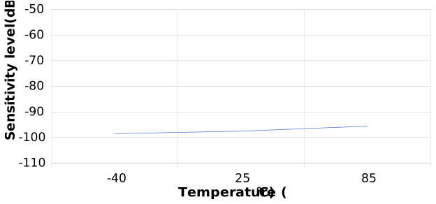
- Bluetooth Low Energy receive sensitivity is measured across temperature at 3.6V, 2440 MHz, uncoded data at 1 Ms/s.
- PDU length = 37
- Sensitivity is measured according to the SIG specifications.
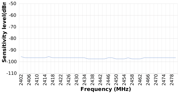
- Bluetooth Low Energy sensitivity is measured across channels at 3.6V at 25℃, uncoded data at 1 Ms/s.
- PDU length = 37
- Sensitivity is measured according to the SIG specifications.
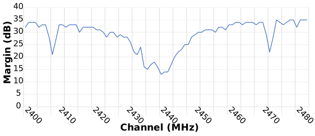
- Bluetooth Low Energy 1M C/I Margin is measured at 2440 MHz at 25℃, 3.6V, uncoded data at 1 Ms/s.
- Reported C/I margin is the margin above the C/I specifications from SIG.
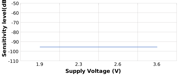
- Bluetooth Low Energy receive sensitivity is measured at 2440 MHz at 25℃, uncoded data at 1 Ms/s.
- PDU length = 37
- Sensitivity is measured according to the SIG specifications.
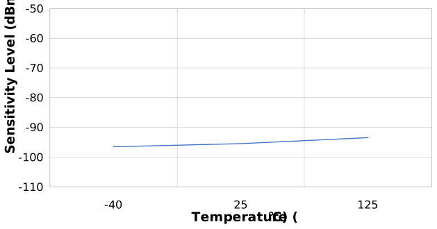
- Bluetooth Low Energy receive sensitivity is measured across channels at 3.6V, 2440 MHz, uncoded data at 1 Ms/s.
- PDU length = 37
- Sensitivity is measured according to the SIG specifications.
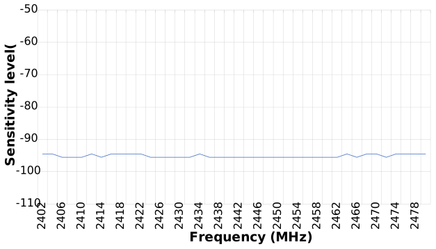
- Bluetooth Low Energy receiver sensitivity is measured across channels at 3.6V at 25℃, uncoded data at 1 Ms/s.
- PDU length = 37
- Sensitivity is measured according to the SIG specifications.
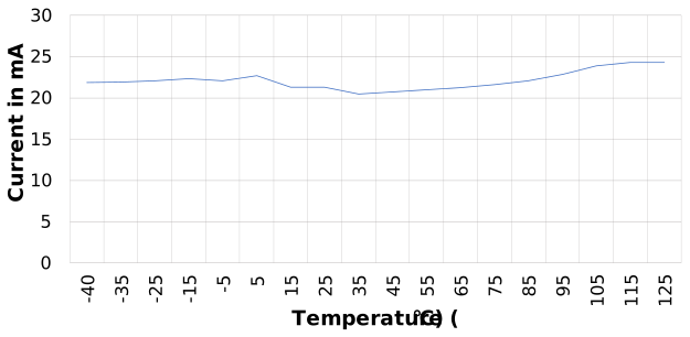
- Bluetooth Low Energy receive current is measured at 3.3V (Buck mode), uncoded data at 1 Ms/s with LNA configured at maximum gain.
- PDU length = 37
- Current is measured on input power rail to SoC (includes processor current as well).
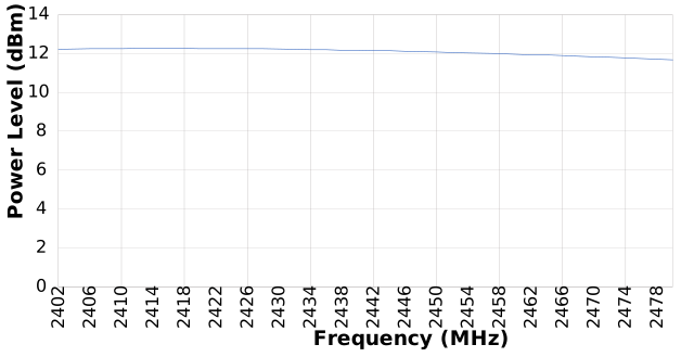
- Bluetooth Low Energy transmit power is measured across frequency after transmit power calibration at 3.3V (Buck mode).
- Transmit power is measured after the PA matching and LPF.
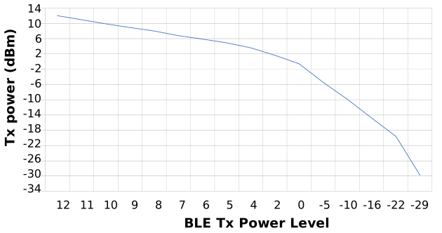
- Bluetooth Low Energy transmit power is measured at 2440 MHz after transmit power calibration.
Transmit power is measured on board based on Microchip Technology Reference Design.
Transmit power is measured after PA match and LPF.
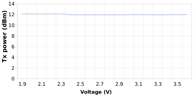
- Bluetooth Low Energy transmit power is measured across voltage after transmit power calibration.
Transmit power is measured after calibration at +12 dBm (± 0.5 dBm).
Transmit power is measured on board based on the Microchip Reference Design.
Transmit power is measured after the LPA and PA match section.
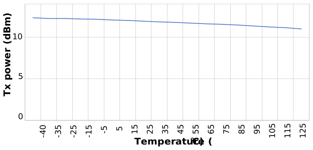
- Bluetooth Low Energy transmit power is measured across temperature after transmit power calibration at 3.6V and 2440 MHz.
- Temperature power compensation is triggered before power measurement.
- Transmit power is measured after the PA matching and LPF.
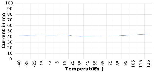
- Bluetooth Low Energy transmit current is measured at 3.3V (Buck mode) at 2440 MHz across temperature.
- Transmit current is measured after calibration at +12 dBm (± 0.5 dBm).
- Current is measured on input power rail to SoC.