
2.2.13 Welcome to FlashROM
FlashROM memory provides secure nonvolatile data storage and includes a 128‑bit AES decryption core. FlashROM contents can be read, modified, and written through the JTAG interface; however, from within the FPGA fabric, FlashROM contents are read‑only.
FlashROM is available from the Catalog in the Libero IDE Project Manager. To use FlashROM, add a FlashROM core from the Catalog to your SmartDesign in the Libero IDE Project Manager. FOr moore information, see the Create/Configure FlashROM section.
FlashROM Capabilities and Applications
GLOO and ProASIC3 devices support flexible programming options. The FlashROM and FPGA fabric can be programmed independently, allowing FlashROM contents to be updated without modifying the FPGA fabric.
Typical applications for FlashROM include:
- Internet Protocol (IP) addressing (wireless or fixed)
- System calibration settings
- Device serialization and inventory control
- Subscription‑based business models (for example, set‑top boxes)
- Secure key storage
- Asset‑management tracking
- Date stamping
- Version management
Programming, Access and Organization
FlashROM is programmed using the standard IEEE 1532 JTAG programming interface. Individual pages can be erased and written independently. The on‑chip AES decryption engine can be selectively enabled to securely load data into FlashROM, such as application‑specific security keys.
For detailed programming instructions, see the FlashPoint Help or the FlashROM User’s Guide.
FlashROM contents can be read either through the JTAG programming interface or through direct FPGA fabric access. Updates to FlashROM contents are permitted only through JTAG.
A 7‑bit address from the FPGA fabric determines:
- The FlashROM page being accessed (3 most‑significant bits),
- The byte within that page (4 least‑significant bits).
Physically, FlashROM is organized as 8 blocks of 128 bits. Logically, it is organized as 8 pages of 16 bytes each.
Only Flash‑based FPGAs include on‑chip nonvolatile memory (NVM). IGLOO, ProASIC3, SmartFusion, and Fusion devices are the FPGA families that support this feature.
You can assign specific regions of FlashROM for dedicated purposes by floorplanning the FlashROM core and assigning properties to those regions.
- If a region is marked as modifiable, its contents can be updated during programming.
- If content modification is not desired, the region can be fixed in SmartDesign.
This allows FlashROM to be partitioned for multiple uses, such as static configuration data, calibration values, or application‑specific storage, while maintaining control over which regions may be updated.
Generated Files
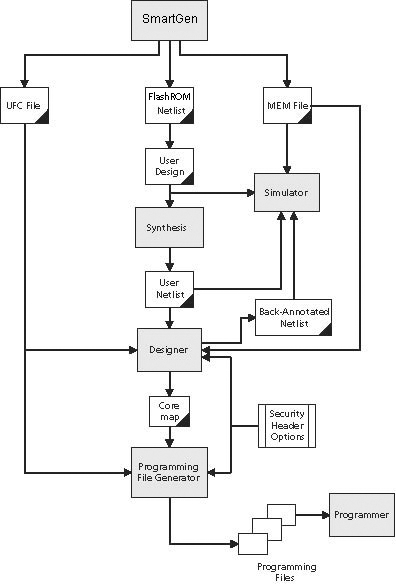
When you generate a FlashROM core, the following files are created and used throughout the design flow:
- CXF file: Contains project information for the Libero IDE.
- Netlist file: Used to instantiate the FlashROM core in your design.
- UFC file (User Flash Configuration file): Contains all configuration information for FlashROM data content and is used during programming. A core‑map file can be combined with the UFC file to generate programming files. Designer software supports importing the UFC file and launching the programming‑file generator.
- MEM file: FlashROM‑specific memory initialization file used exclusively for simulation. The MEM file contains 128 rows of 8‑bit values. Unspecified FlashROM locations default to 0.
FlashROM Design Flow Support
- Configure FlashROM
- Simulate Pre/Post Synthesis
- Synthesize
- Place-and-Route
- Run Back-Annotation and Timing Simulation
- Specify security settings
- Specify FlashROM content
- Generate a programming file