
2.2.10 Configuring Current, Differential Voltage, Temperature, and Voltage peripherals
The Current, Differential Voltage, Temperature, and Voltage peripherals are configured using the same basic options. The effects of averaging are also identical for all peripherals in the Analog System Builder (ASB).
Minor variations, such as Maximum Voltage for the Voltage Monitor,, are described in the help topic for the corresponding peripheral.
- Signal Name
Specifies the name of the signal as it appears in the main Analog System Builder dialog box and in the generated design outputs.
- Digital Filtering
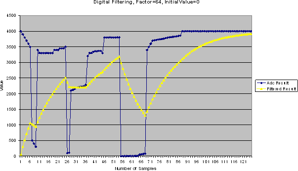
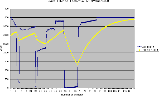
After the ADC completes a conversion, the resulting digital value can be filtered (averaged). Digital filtering is implemented as a single‑pole low‑pass filter using soft logic and can be used to improve the signal‑to‑noise ratio. If the ADC input signal is noisy or erratic, digital filtering smooths the input and reduces noise.
The filtered value is calculated using the following equation:
FilteringResultₙ = FilteringResultₙ₋₁ + (ADCResultₙ / FilteringFactor)− (FilteringResultₙ₋₁ / FilteringFactor)
If the Digital Filtering Factor is set to 1, filtering is effectively disabled.
In applications where the input signal has a very low frequency and the electrical environment is relatively noise‑free, filtering may not be required. However, in most applications it is desirable to implement at least basic post‑conversion digital filtering by oversampling and averaging multiple ADC results to reduce random noise and improve accuracy.
This averaging is automatically handled by ASB. When the filtering factor is set to F, F samples are averaged together.
For applications requiring higher accuracy, an external analog filter may be necessary to suppress non‑random and out‑of‑band noise sources. Without such filtering, out‑of‑band signals may alias into the conversion result as in‑band noise. Some applications, such as frequency detection, may require both external analog filtering and more advanced digital filtering (for example, a multi‑tap FIR filter), which can be implemented using FPGA logic.
- Initial Filtering Value
The Initial Filtering Value specifies the starting value for the averaging function (FilteringResult[0]). This allows the filtering operation to be seeded so that invalid values are not produced during startup.
If no initial filtering value is specified, the filter starts with FilteringResult[0] = 0, which biases the early results toward zero.
The valid range for the initial filtering value is identical to the threshold range of the associated peripheral. for more information, see the ASB - Calculating a Threshold section.
The system instantiates averaging logic as soon as at least one channel requires filtering. No additional logic penalty is incurred when filtering is enabled for other channels.
- Acquisition Time
The acquisition time specifies the required settling and sampling time for the input channel. It represents the time required for the ADC sample‑and‑hold circuit to charge its capacitor with the input analog signal.
The required acquisition time depends on system characteristics and monitoring requirements and has a direct impact on the maximum achievable sampling rate.
The prescaler logic in the analog block (AB) has a maximum settling time of 10 µs (see the Prescaler Rogic section). This settling time is application‑dependent and must be included in the acquisition and hold time configuration for each channel. ASB inserts a recommended default value when configuring a new Voltage Monitor; this value may be reduced at the cost of reduced sampling accuracy.
ASB evaluates the acquisition times of all peripherals along with the system frequency to compute the maximum possible ADC clock frequency. Because only certain divider values are available for ADC clock generation, some system clock frequencies result in higher ADC clock rates than others.
- Signal Polarity
Applies to current and differential voltage peripherals only.
This option specifies the polarity of the measurement. The associated Voltage Monitor must be configured with the same polarity. During simulation, a negatively configured peripheral must be driven with negative voltage values.
- Comparison Flag Specification
- Click Add Flag to create a new flag.
- Select a flag and click Delete to remove it.
- Flag Name
Specifies the name of the flag. This name appears as an output port in the generated design and is prefixed with the associated signal name.
- Flag Type
Specifies whether the flag asserts when the signal value is above or below the specified threshold.
- Threshold
Specifies the threshold value used for comparison. Figure 30 illustrates the effect of a threshold on a signal.
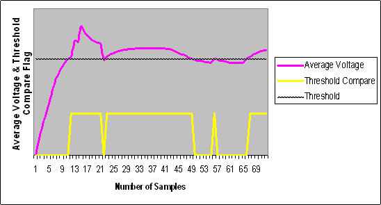
- Assert Samples
Specifies the number of consecutive samples that must meet or exceed the threshold before the flag asserts. This provides glitch‑removal functionality. If set to 1, the flag behavior directly reflects the comparison result.
For example, if Assert Samples is set to 5 and the threshold is 3.0V, the signal must reach or exceed 3.0V for five consecutive samples for the flag to assert.
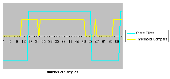
- De‑assert Samples
Specifies the number of consecutive samples that must fall below the threshold for the flag to de‑assert after being asserted. This also provides glitch‑removal functionality. If set to 1, the flag behavior directly reflects the comparison result.
For example, if De‑assert Samples is set to 10 and the threshold is 3.3V, the signal must remain below 3.3V for ten consecutive samples before the flag de‑asserts.