
14.8.22 RF_CTRL_0
| Name: | RF_CTRL_0 |
| Offset: | 0x16 |
| Reset: | 0x31 |
| Property: | - |
| Bit | 7 | 6 | 5 | 4 | 3 | 2 | 1 | 0 | |
| PA_LT[1:0] | GC_TX_OFFS[1:0] | ||||||||
| Access | R/W | R/W | - | - | - | - | R/W | R/W | |
| Reset | 0 | 0 | 1 | 1 | 0 | 0 | 0 | 1 | |
Bits 7:6 – PA_LT[1:0] PA_LT
This bit control lead time of the PA (relative to first chip of TX data).
| Value | Description |
|---|---|
| 0x0 | 2μs |
| 0x1 | 4μs |
| 0x2 | 6μs |
| 0x3 | 8μs |
These register bits control the lead time of the PA enable signal relative to the TX data start. This allows to enable the PA 2, 4, 6, or 8μs before the transmit signal starts. The PA enable signal can also be output at differential pin pair DIG3/DIG4 to provide a control signal for an external RF front-end.
Bits 1:0 – GC_TX_OFFS[1:0] GC_TX_OFFS
The register bits GC_TX_OFFS control the TX power offset.
| Value | Description |
|---|---|
| 0x0 | Reserved |
| 0x1 | 0dB |
| 0x2 | +1dB |
| 0x3 | +2dB |
These register bits provide an offset between the TX power control word TX_PWR (register 0x05, PHY_TX_PWR) and the actual TX power. This 2-bit word is added to the TX power control word before it is applied to the circuit block which adjusts the TX power. It can be used to compensate differences of the average TX power depending of the modulation format.
| Mode | BPSK | O-QPSK |
|---|---|---|
| GC_TX_OFFS | 0x3 | 0x2 |
Exception for OQPSK-RC-{100,200,400}, see Table 14-54
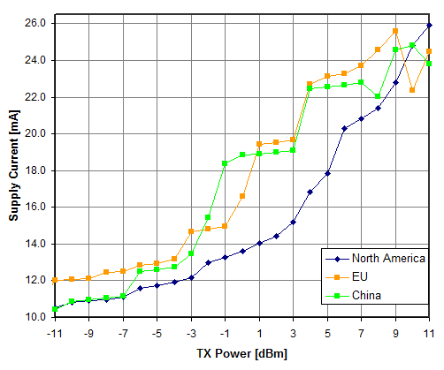
The North American mapping table is optimized for lowest supply current. The more relaxed spectral side lobe requirements of the IEEE 802.15.4 standard are fulfilled.
The European mapping tables take into account that linearity is needed to keep the out-of-band spurious emissions below the ETSI requirements, refer to [6]. Regulatory requirements with respect to power density (depending on the frequency band used) are not considered, refer to [7].
The European mapping takes more supply current than the North American map and uses the normal (linearized) PA mode to provide medium output power up to 3dBm for OQPSK-SIN-RC-{100/200/400} modes and 6dBm for BPSK-20 mode.
The Chinese mapping uses the boost mode to provide higher TX power levels at the expense of higher supply current. As a result, the maximum TX power is 11dBm for OQPSK-RC-{250/500) modes.
Due to great regional distinctions of regulatory requirements, it is not possible to cover all restrictions in this datasheet. Manufactures must take the responsibility to check measurement results against the latest regulations of nations into which they market.