49.21 SPI Module Electrical Specifications
| AC Characteristics | Standard Operating Conditions: VDD33 =
VDDIO = AVDD = 1.9–3.6V (Unless Otherwise Stated) Operating Temperature: -40°C ≤ TA ≤ +125°C for Extended Temperature | ||||||
|---|---|---|---|---|---|---|---|
| Parameter Number | Symbol | Characteristics | Min. | Typ. | Max. | Units | Conditions |
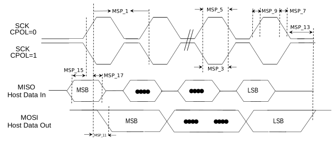
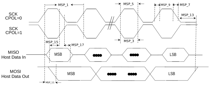
| MSP_1 | FSCK | SCK Frequency | — | — | 16 | MHz | VDDIO = 3.3V, CLOAD = 30 pF(MAXIMUM) DIRECT pins |
| — | — | 10.67 | VDDIO = 3.3V, CLOAD = 30 pF(MAXIMUM) Remappable pins | ||||
| — | — | 16 | VDDIO = 1.9V, CLOAD = 30 pF(MAXIMUM) DIRECT pins | ||||
| — | — | 10.67 | VDDIO = 1.9V, CLOAD = 30 pF(MAXIMUM) Remappable pins | ||||
| MSP_3 | TSCL | SCK Output Low Time | — | 1/(2×FSCK) | — | ns | — |
| MSP_5 | TSCH | SCK Output High Time | — | 1/(2×FSCK) | — | ns | — |
| MSP_7 | TSCF | SCK and MOSI Output Fall Time | — | — | DI27 | ns | See DI27 parameter in the I/O Pin AC/DC Electrical Specifications table in the I/O Pin AC/DC Electrical Specifications from Related Links |
| MSP_9 | TSCR | SCK and MOSI Output Rise Time | — | — | DI25 | ns | See DI25 parameter in the I/O Pin AC/DC Electrical Specifications table in the I/O Pin AC/DC Electrical Specifications from Related Links |
| MSP_11 | TMOV | MOSI Data Output Valid after SCK | — | — | 7 | ns | DIRECT pins |
| — | — | 13 | ns | Remappable/PPS pins | |||
| MSP_13 | TMOH | MOSI hold after SCK | 5 | — | — | ns | — |
| MSP_15 | TMIS | MISO Setup Time of Data Input to SCK | 27 | — | — | ns | DIRECT pins |
| 35 | — | — | ns | Remappable/PPS pins | |||
| MSP_17 | TMIH | MISO Hold Time of Data Input to SCK | 0 | — | — | ns | — |
| MSP_19 | SPI_GCLK | SERCOM SPI input clk freq, GCLK_SPI | — | — | FCLK_67 | MHz | — |
|
Note:
| |||||||
| AC Characteristics | Standard Operating Conditions: VDD33
= VDDIO = AVDD = 1.9–3.6V (Unless Otherwise Stated) Operating Temperature: -40°C ≤ TA ≤ +125°C for Extended Temperature | ||||||
|---|---|---|---|---|---|---|---|
| Parameter Number | Symbol | Characteristics(1, 2) | Min. | Typical | Max. | Units | Conditions |
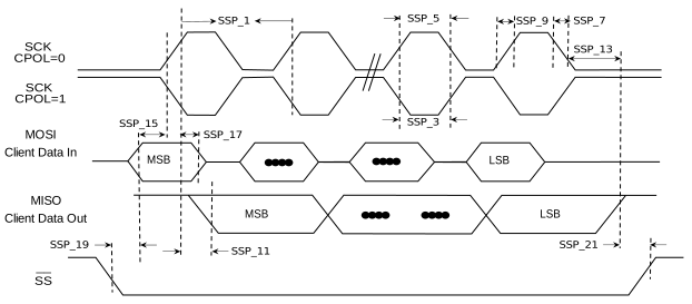
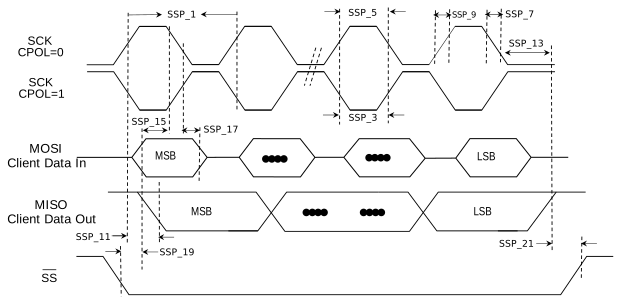
| SSP_1 | FSCK | SCK Frequency | — | — | 16 | MHz | VDDIO = 3.3V, CLOAD = 30 pF(MAXIMUM) DIRECT pins |
| — | — | 10.67 | VDDIO = 3.3V, CLOAD = 30 pF(MAXIMUM) Remappable pins | ||||
| — | — | 16 | VDDIO = 1.9V, CLOAD = 30 pF(MAXIMUM) DIRECT pins | ||||
| — | — | 10.67 | VDDIO = 1.9V, CLOAD = 30 pF(MAXIMUM) Remappable pins | ||||
| SSP_3 | TSCL | SCK Output Low Time | — | 1/(2×FSCK) | — | ns | — |
| SSP_5 | TSCH | SCK Output High Time | — | 1/(2×FSCK) | — | ns | — |
| SSP_7 | TSCF | MISO Output Fall Time | — | — | DI27 | ns | See DI27 parameter in the I/O Pin AC/DC Electrical Specifications table in the I/O Pin AC/DC Electrical Specifications from Related Links |
| SSP_9 | TSCR | MISO Output Rise Time | — | — | DI25 | ns | See DI25 parameter in the I/O Pin AC/DC Electrical Specifications table in the I/O Pin AC/DC Electrical Specifications from Related Links |
| SSP_11 | TSOV | MISO Data Output Valid after SCK | — | — | 24 | ns | DIRECT pins |
| — | — | 34 | ns | Remappable/PPS pins | |||
| SSP_13 | TSOH | MISO hold after SCK | 0 | — | — | ns | — |
| SSP_15 | TSIS | MOSI Setup Time of Data Input to SCK | 6 | — | — | ns | DIRECT pins |
| 7 | — | — | ns | Remappable/PPS pins | |||
| SSP_17 | TSIH | MOSI Hold Time of Data Input to SCK | 1 | — | — | ns | DIRECT pins |
| 2 | — | — | ns | Remappable/PPS pins | |||
| SSP_19 | TSSS | SS setup to SCK (PRELOADEN = 1) | TSCK+13 | — | — | ns | — |
| SS setup to SCK (PRELOADEN = 0) | TSCK | — | — | ns | — | ||
| SSP_21 | TSSH | SS hold after SCK Client | TSIH-1 | — | — | ns | — |
| SSP_23 | SPI_GCLK | SERCOM SPI input clk freq, GCLK_SPI | — | — | FCLK_67 | MHz | — |
|
Note:
| |||||||