49.14 XOSC32 (SOSC) AC Electrical Specifications

Table 49-15. XOSC32 (SOSC) AC Electrical Specifications
AC CharacteristicsStandard Operating Conditions: VDD33 = VDDIO = AVDD = 1.9–3.6V (Unless Otherwise Stated)

Operating Temperature:

-40°C ≤ TA ≤ +125°C for Extended Temperature

Parameter NumberSymbolCharacteristicsMin.Typ.(1)Max.UnitsConditions
XOSC32_1FOSC_XOSC32XOSC32 Oscillator Crystal Frequency—32.768—kHzXIN32, XOUT32 Secondary Oscillator ± 250 ppm
XOSC32_3CXIN32XOSC32 XIN32 parasitic pin capacitance (PIC32CX-BZ6)—4.6—pF—
XOSC32 XIN32 parasitic pin capacitance (PIC32WM-BZ6)—5.2—pF—
XOSC32_5CXOUT32XOSC32 XOUT32 parasitic pin capacitance (PIC32CX-BZ6)—4.3—pF—
XOSC32 XOUT32 parasitic pin capacitance (PIC32WM-BZ6)—5.1—pF—
XOSC32_11CLOAD_X32(3)32.768 kHz Crystal Load Capacitance—11 —pF—
XOSC32_12—— —pF—
XOSC32_13ESR_X3232.768 kHz Crystal ESR—75100KΩ—
XOSC32_14—— —Ω—
XOSC32_15TOSC32TOSC32 = 1/FOSC_XOSC32—30.518—µsSee parameter XOSC32_1 for FOSC_XOSC32 value
XOSC32_17XOSC32_ST (2)XOSC32 Crystal Start-up Time —206 317msFrom clock request to Oscillator Ready
Note:
  1. Typical value tested but not characterized.
  2. This is for guidance only. A major component of crystal start-up time is based on the second party crystal MFG parasitic that is outside the scope of this specification. If this is a major concern, the customer might need to characterize this based on their design choices.
  3. The test conditions for the crystal load capacitor calculation are as follows:
    • Standard PCB trace capacitance = 1.5 pF per 12.5 mm (0.5 inches) (in other words, PCB STD TRACE W = 0.175 mm, H = 36 μm, T = 113 μm)
    • Xtal PCB capacitance typical; therefore, ~= 2.5 pF for a tight PCB xtal layout
    • For CXIN and CXOUT within 4 pF of each other, assume CXTAL_EFF = ((CXIN+CXOUT)/2)
    • Note: Averaging CXIN and CXOUT will affect the final calculated CLOAD value by less than the tolerance of the capacitor selection.
    Equation 1:
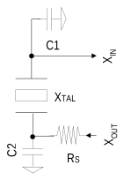
    MFG   CLOAD⁢  Spec = {([CXIN⁢ +  C1]  *  [CXOUT⁢   +  C2])/[CXIN⁢ +  C1⁢ +C2⁢ +CXOUT]}  + estimated⁢ oscillator⁢ PCB⁢ stray⁢ capaci⁢tance⁢

    Assuming C1 = C2 and CXin ~= CXout, the formula can be further simplified and restated to solve for C1 and C2 by:

    Equation 49-3. Equation 2 (In other words: Simplified Equation 1)
    C1⁢  =   C2⁢  =  ((2⁢ *  MFG   CLOAD⁢  Spec)  −CXTAL_EFF⁢ −  (2⁢ *  ⁢ PCB⁢   ⁢ capaci⁢tance))⁢

    Example:

    • XTAL Mfg CLOAD Data Sheet Spec = 12 pF
    • PCB XTAL trace Capacitance = 2.5 pF
    • CXIN pin = 6.5 pF, CXOUT pin = 4.5 pF therefore CXTAL_EFF = ((CXIN+CXOUT)/2)

    CXTAL_EFF = ((6.5 + 4.5)/2) = 5.5 pF

    C1 = C2 = ((2 * MFG Cload spec) – CXTAL_EFF – (2 * PCB capacitance))

    C1 = C2 = (24 – 5.5 – (2 * 2.5))

    C1 = C2 = (24 – 5.5 – 5)

    C1 = C2 = 13.5 pF (Always rounded down)

    C1 = C2 = 13 pF (in other words, for hypothetical example crystal external load capacitors)

    User C1 = C2 = 13 pF ≤ CLOAD_X32 (maximum) specification

Figure 49-17. XOSC32 Block Diagram