
14.8.249 GNAND2
This component is supported by ACT 1, ACT 2, ACT 3, 3200DX, MX, SX, SX-A, SX-S, eX, Accelerator families.
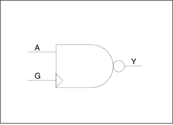
- Function: 2-Input NAND Clock Net
- Input: A, G
- Output: Y
| A | G | Y |
|---|---|---|
| X | 0 | 1 |
| 0 | X | 1 |
| 1 | 1 | 0 |
| Family | Seq | Comb |
|---|---|---|
| All | — | 1 |
Note: G pin can be connected directly to a routed clock (RCLK) or hardwired clock (HCLK) if supported by your device. See your device datasheet for more info.